Unlock instant, AI-driven research and patent intelligence for your innovation.

Photodetector and unit mounted with photodetector

a photodetector and photodetector technology, applied in the field of photodetectors and units mounted with photodetectors, can solve the problems of difficult to diffuse impurities deeply, with good control, and fluctuations in the composition of ingaasps, and achieve easy flip-chip bonding, reduce parasitic capacitance, and high operation speed

Inactive Publication Date: 2005-06-21
PANASONIC CORP
View PDF12 Cites 6 Cited by
  • Summary
  • Abstract
  • Description
  • Claims
  • Application Information

AI Technical Summary

Benefits of technology

"The present invention provides a photodetector with long wavelength passband properties that has a high sensitivity ratio even with a thin filter layer. The photodetector has a filter layer with an absorption edge wavelength longer than the absorption edge wavelength of the semiconductor substrate and shorter than the absorption edge wavelength of the light absorption layer. The depth of impurity diffusion is equivalent to conventional PIN photodiodes. The photodetector can be easily made with flip-chip bonding and has a reduced size difference between the light absorption layer and the diffusion region. The first photodetector includes a reflective film and a carrier blocking layer. The second photodetector includes a sloped portion for reflecting incident light. The third photodetector includes a wide band gap layer with an impurity diffusion region. The fourth photodetector includes a sloped portion and a wide band gap layer with an impurity diffusion region."

Problems solved by technology

However, there is the problem that epitaxially growing a thick InGaAsP easily causes fluctuations in the composition of the InGaAsP.
This means that in conventional PIN photodiodes, even taking InGaAsP as the material for the filter layer 105 and being able to epitaxially grow the filter layer 105 thickly leaves the problem that it is difficult to diffuse impurities deeply and with good control.

Method used


Image

  • Photodetector and unit mounted with photodetector
  • Photodetector and unit mounted with photodetector
  • Photodetector and unit mounted with photodetector

Examples


first embodiment

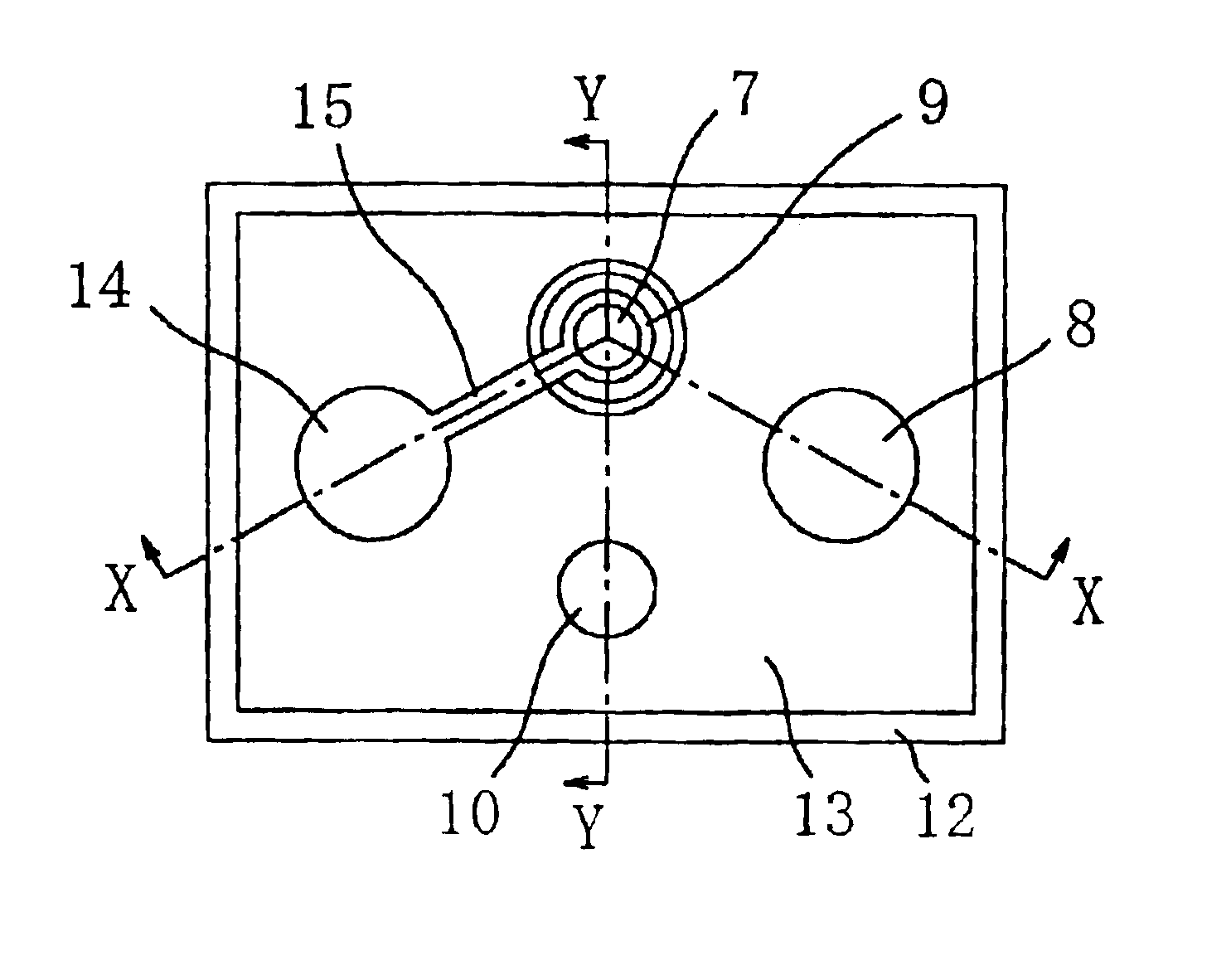
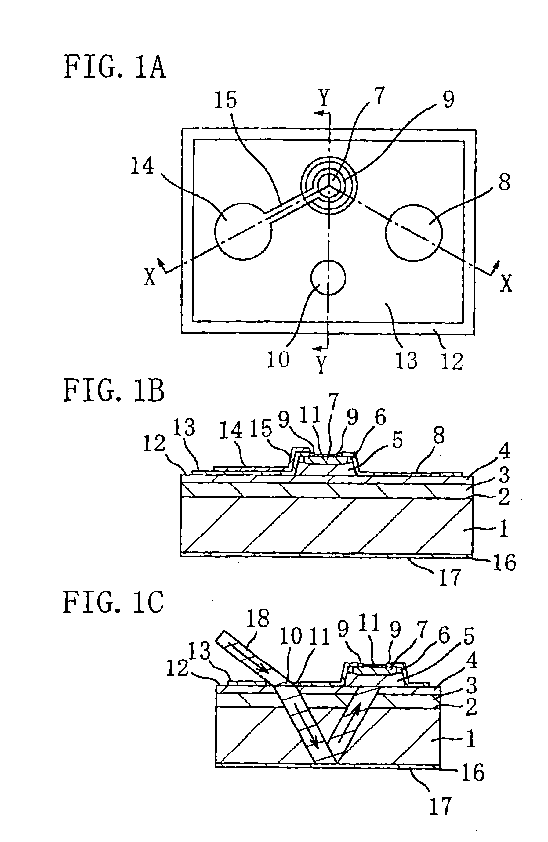
[0068]The photodetector according to a first embodiment of the present invention will be described with reference to FIG. 1. FIG. 1A is a plan view of the photodetector according to the first embodiment. FIG. 1B is a cross-sectional view taken along the X—X line in FIG. 1A. FIG. 1C is a cross-sectional view taken along the Y—Y line in FIG. 1A.

[0069]The photodetector of this embodiment includes a semiconductor substrate 1, a filter layer 3 formed on a first principal face 2 of the semiconductor substrate 1, and a light absorption layer 5 formed in an island on the filter layer 3. Here the absorption edge wavelength of the filter layer 3 is longer than the absorption edge wavelength of the semiconductor substrate 1 and shorter than the absorption edge wavelength of the light absorption layer 5. Further, a light incidence portion 10 is formed at a portion of the filter layer 3 where the light absorption layer 5 has not been formed. It is preferable that a carrier blocking layer (buffer...

second embodiment

[0096]The photodetector according to a second embodiment of the present invention will be described with reference to FIG. 4. FIG. 4A is a plan view of the photodetector according to the second embodiment, FIG. 4B is a cross-sectional view taken along the X—X line in FIG. 4A, and FIG. 4C is a cross-sectional view taken along the Y—Y line in FIG. 4A. FIG. 4D is a rear face view showing the shape of the spot of a sloped portion 19 when the semiconductor substrate 1 is viewed from its rear face.

[0097]As shown in FIG. 4C, the feature where the photodetector according to the second embodiment differs from the photodetector according to the first embodiment is that an indented portion with the sloped portion 19 is formed in the second principal face 16 of the semiconductor substrate 1, and a reflective film 20 is formed on the second principal face 16 of the semiconductor substrate 1 having the sloped portion 19. It should be noted that the incident light 18 is incident to the sloped port...

third embodiment

[0101]The photodetector according to a third embodiment of the present invention will be described with reference to FIG. 5. FIG. 5A is a plan view of the photodetector according to the third embodiment, FIG. 5B is a cross-sectional view taken along the X—X line in FIG. 5A, and FIG. 5C is a cross-sectional view taken along the Y—Y line in FIG. 5A.

[0102]As shown in FIG. 5C, the feature where the photodetector according to the third embodiment differs from the photodetector according to the first embodiment is that the filter layer 3 is not formed on the first principal face 2 of the semiconductor substrate 1 and instead a filter layer 21 is formed on the second principal face 16 of the semiconductor substrate 1, and the reflective film 17 is formed on the filter layer 21. Also, another feature is that the carrier blocking layer is not formed.

[0103]For the sake of simplifying the description, the same components as those of the photodetector of the first embodiment bear the same numer...


PUM


Abstract

A filter layer and a buffer layer are sequentially laminated on a first principal face of a semiconductor substrate, and an island-shaped light absorption layer and a window layer are laminated on top of the buffer layer. A diffusion region in which p-type impurities have been diffused is formed in the window layer. An n-side electrode and a p-side electrode are formed on the buffer layer and the diffusion region, respectively. A light incidence portion is formed on the buffer layer where the light absorption layer has not been formed.

Description

BACKGROUND OF THE INVENTION[0001]The present invention relates to a photodetector and a unit mounted with a photodetector, and in particular relates to a photodetector that selectively receives signal light of a long wavelength (on the long wavelength side) when there is a plurality of incident signal lights of different wavelengths.[0002]Currently there are broad applications for PIN photodiodes of a compound semiconductor material as photodetectors for optical fiber communications.[0003]These PIN photodiodes employ a window structure to increase light-receiving sensitivity. In these PIN photodiodes, a light absorbing layer with a small forbidden bandwidth (long absorption edge wavelength) is formed on a semiconductor substrate, and a filter layer (window layer) with a large forbidden bandwidth (short absorption edge wavelength) is formed thereon. This structure makes it possible for light of the absorption edge wavelengths of the light absorption layer and the filter layer to be e...

Claims


Application Information

Patent Timeline
Patent Type & Authority Patents(United States)
IPC IPC(8): H01L31/00H01L31/0328H01L31/109
CPCH01L31/02162H01L31/0203
Inventor MATSUDA, KENICHI
Owner PANASONIC CORP