Semiconductor light emitting device with reflectors having cooling function

a technology of light emitting device and reflector, which is applied in the manufacture of semiconductor/solid-state devices, semiconductor devices, electrical devices, etc., can solve the problems of shortening the life of leds and deteriorating sealing resins or fluorescent substances, and achieve excellent thermal conductivity and good reflective ratio

Inactive Publication Date: 2005-06-21
HIGH POWER LIGHTING CORP
View PDF15 Cites 63 Cited by
  • Summary
  • Abstract
  • Description
  • Claims
  • Application Information

AI Technical Summary

Benefits of technology

[0013]Therefore, it is an object of the present invention to provide a light emitting device in which a reflector surrounding a light emitting element is made of a material having excellent thermal conductivity as well as good reflective ratio so that the reflector may radiate heat generated in the LED chip to outside.
[0015]In addition, still another object of the invention is to improve the uniformity of light by forming a concave reflective surface in an inner side of the reflector.
[0017]In addition, the inventors was also acquainted with the fact that it is possible to improve the light output when silicate having good translucency is used for the sealing resin for covering the LED chip.

Problems solved by technology

The inventors was acquainted with the facts that when a side wall is formed around a surface-mounted LED chip to realize strobe light, the heat generated in the LED chip is not effectively emitted outside, thereby shortening the life of the LED and deteriorating the sealing resin or fluorescent substances.

Method used


Image

  • Semiconductor light emitting device with reflectors having cooling function
  • Semiconductor light emitting device with reflectors having cooling function
  • Semiconductor light emitting device with reflectors having cooling function

Examples


modified example 1

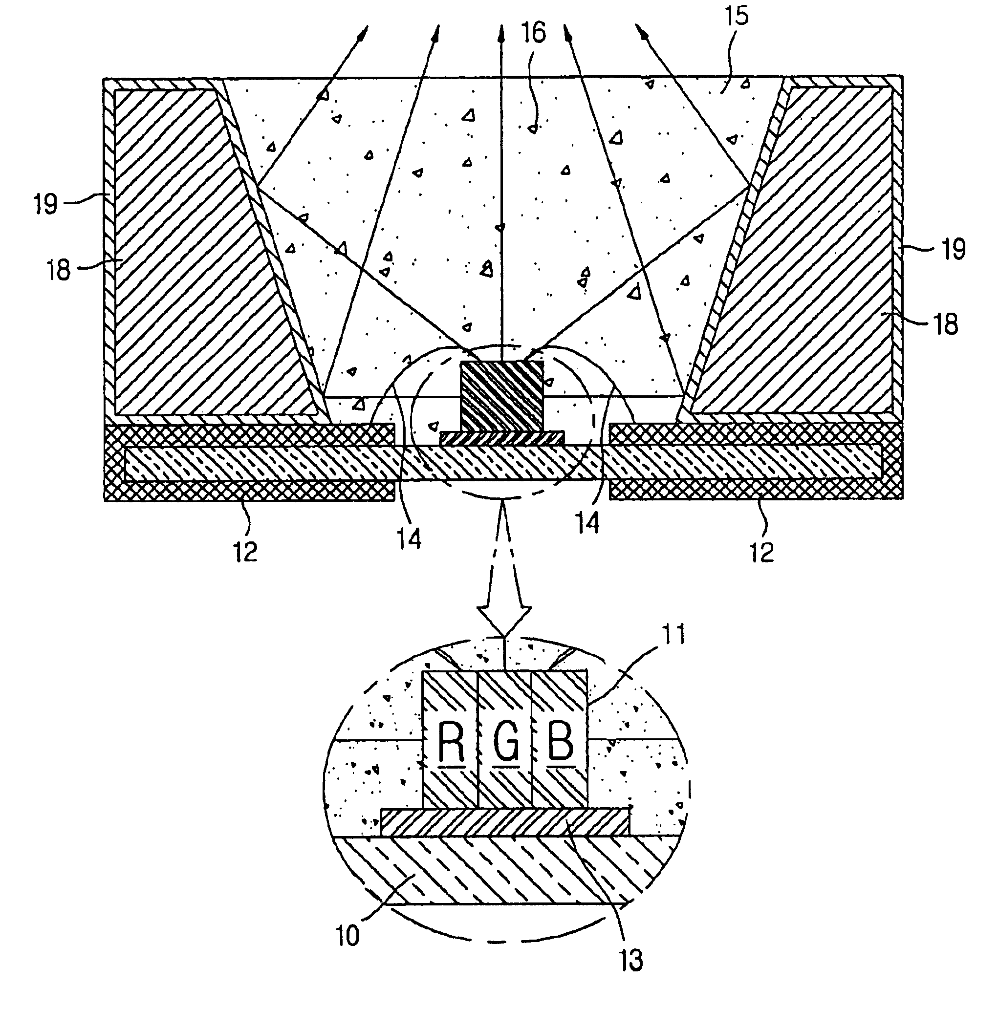
[0052]In this modified example, at least one blue light emitting diode, at least one red light emitting diode and at least one green light diode are formed into an assembly and then this assembly is mounted on the base substrate 10 in the receiving space formed by the reflector 18, differently from the first embodiment in which only blue light emitting diode are mounted in the receiving space. This modification is illustrated in the inset diagram of FIG. 1.

[0053]In other words, the light emitting device of this modified example realizes white light by combination of the red-, blue- and green-light (i.e., R-G-B combination) emitted from the red-, blue- and green-light emitting diodes. Thus, this modified example does not require to mix any color-shifting substance 16 such as a fluorescent material into the sealing resin 15 charging the inside of the receiving space as in the case of the first embodiment.

[0054]The red-, blue- and green-light emitting diodes composing the assembly may ...

modified example 2

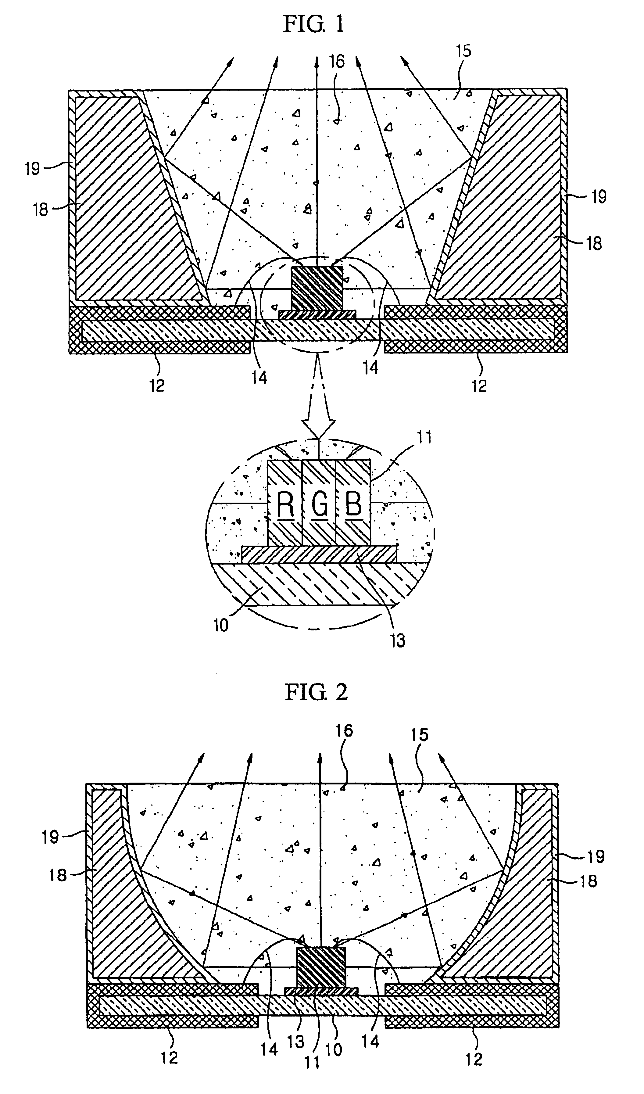
[0062]This modified example is substantially identical to the second embodiment, except that the light emitting diode assembly is disposed in the receiving space, and the transparent sealing resin not mixed with the color-shifting material is used like the modified example 1.

[0063]Third Embodiment

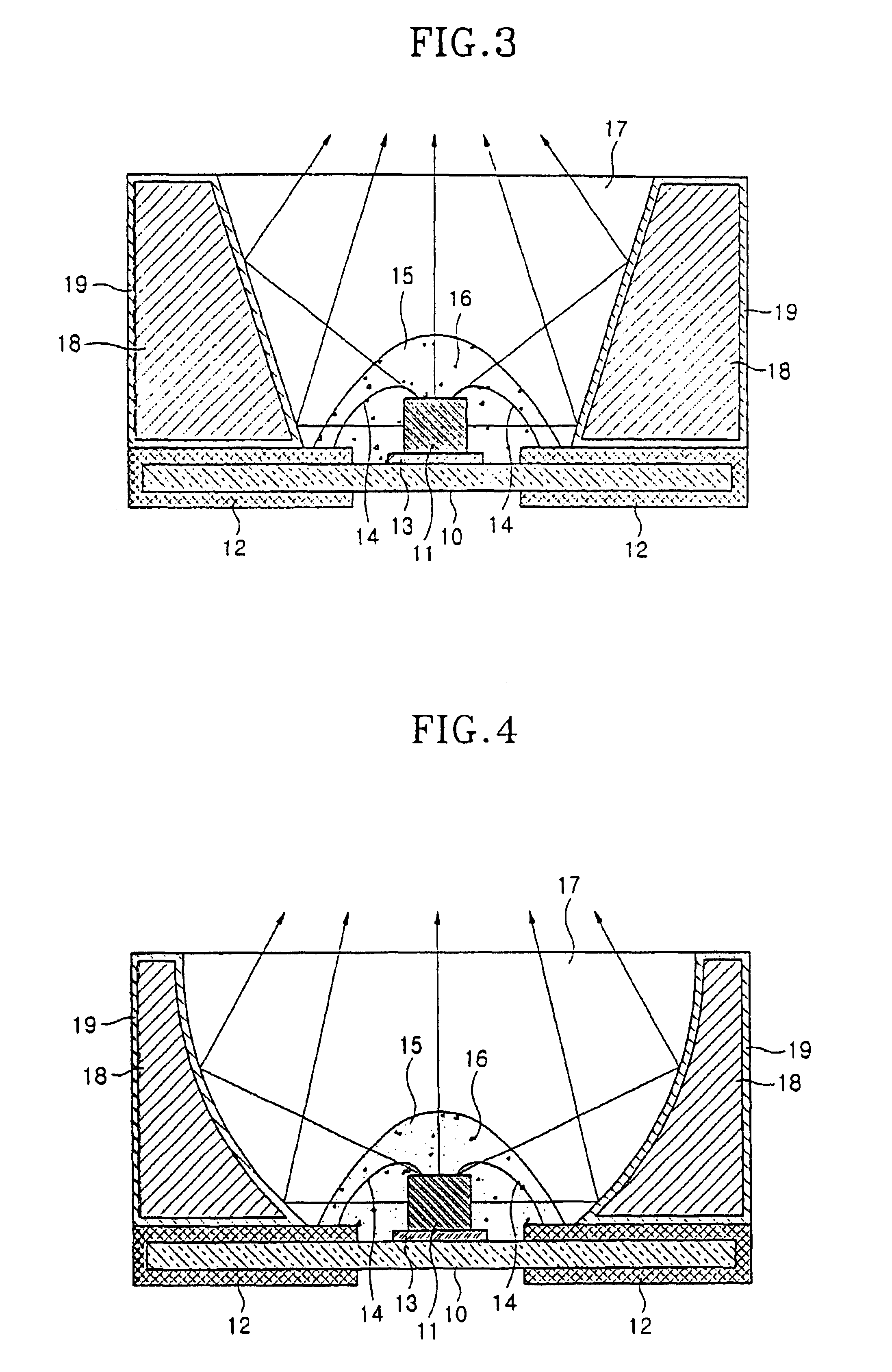
[0064]FIG. 3 shows a semiconductor light emitting device according to a third embodiment of the present invention.

[0065]The light emitting device of this embodiment is substantially identical to the first embodiment, except the configuration of translucent cover layers 15 and 17. Thus, the following description is mainly focused on the configuration of the translucent cover layers 15 and 17, differently from the first embodiment, and other components are not described in detail.

[0066]As shown in FIG. 3, the translucent cover layers 15 and 17 are formed in two stages, differently from the sealing resin 15 of the first embodiment.

[0067]First Translucent Cover Layer (15)

[0068]The first translu...


PUM


Abstract

A semiconductor light emitting device includes a base substrate, lead electrodes provided on the base substrate, at least one semiconductor light emitting element loaded on the base substrate so as to be spaced apart from the lead electrodes and radiating blue light, a connection member for electrically interconnecting the electrodes and the semiconductor light emitting element, a reflector extended from a bottom of the base substrate to a predetermined height for surrounding the semiconductor light emitting element, and a translucent cover layer formed in the receiving space for housing the light emitting element, the translucent cover layer containing a color-shifting substance for absorbing at least a part of blue light radiated from the light emitting element to radiate a light having a different wavelength. The reflector is made of a material having high translucency and high thermal conductivity on a surface thereof so as to reflect the light radiated from the light emitting element and form a uniform planar light, and the reflector radiates the heat radiated from the light emitting element to outside so as to cool an inside of a receiving space for receiving the light emitting element. Thus, the device emits white light outside by combination of the blue light radiated from the light emitting element and the light having a different wavelength.

Description

BACKGROUND OF THE INVENTION[0001]1. Field of the Invention[0002]The present invention relates to a semiconductor light emitting device for emitting white light, and more particularly to a semiconductor light emitting device provided with a reflector for radiating heat generated in light emitting elements to outside.[0003]2. Description of the Related Art[0004]Nowadays, there is developed a light emitting diode (LED) chip using a gallium nitride semiconductor, which may emit blue light of high brightness. When using this gallium nitride semiconductor, the LED has a large output and less color shift in comparison with other LEDs emitting red light or yellowish-green light.[0005]This blue light emitting diode chip is broadly used in various devices such as portable electronic equipment, a sign lamp or an indication lamp. To apply the LED chip to the above-mentioned devices, a point emission should be converted into a planar emission.[0006]For this reason, in the prior art, a chip is in...

Claims


Application Information

Patent Timeline
Patent Type & Authority Patents(United States)
IPC IPC(8): H01L33/00H01L33/32H01L33/44H01L33/50H01L33/56H01L33/60H01L33/62H01L33/64
CPCH01L33/486H01L33/44H01L33/50H01L33/60H01L2224/48091H01L2224/48227H01L2224/45144H01L2224/92247H01L2924/00014H01L2924/00
Inventor HAYASHIMOTO, YOSHIAKISEO, YOUNG-JOO
Owner HIGH POWER LIGHTING CORP
Why Eureka
Try Eureka