Supercharge Your Innovation With Domain-Expert AI Agents!

Resin encapsulation semiconductor device utilizing grooved leads and die pad

a technology of grooved leads and die pads, which is applied in the direction of casings/cabinets/drawers, electrical apparatus construction details, casings/cabinets/drawers details, etc., can solve the problems of affecting the encapsulation of the semiconductor device, and affecting the reliability of the connection, so as to reduce the thickness and reduce the chip area ratio , the effect of small thickness

Inactive Publication Date: 2005-06-21
TESSERA ADVANCED TECH
View PDF12 Cites 22 Cited by
  • Summary
  • Abstract
  • Description
  • Claims
  • Application Information

AI Technical Summary

Benefits of technology

"The resin-encapsulation semiconductor device described in this patent has several technical effects. First, the device includes a thin portion on the tips of the leads, which helps to reduce the thickness of the device. Second, the device has a groove on the outer edge of the die pad, which helps to position the semiconductor element accurately. Third, the device has metal wires connected to the semiconductor element, which are connected to the leads in a way that reduces the risk of short circuits. Fourth, the device has a thin portion on the tips of the leads, which helps to reduce the thickness of the device. Fifth, the method for fabricating the device includes steps of preparing a lead frame, mounting a semiconductor element on the lead frame, and resin encapsulating the lead frame, which simplifies the manufacturing process."

Problems solved by technology

In particular, when a large semiconductor element is packaged, the thickness of the resin-encapsulation semiconductor device is greatly affected, and hence, it is impossible to attain, by using this structure, a small thickness with a large semiconductor element packaged.
Furthermore, the inner leads are encapsulated substantially on the single side, and hence, external impact or stress caused within the encapsulation resin may apply stress to the metal wires connected onto the inner leads, so that there may be fear of break and degradation of the reliability in the connection.
However, in consideration of the area of each lead included in a small package, it is very difficult to form a plurality of grooves on each inner lead and further secure a bonding area for the connection to a metal wire.
Therefore, in order to separate each resin-encapsulation semiconductor device from the lead frame after the encapsulation, it is necessary to cut the lead frame with a mold, which can be an obstacle to improve the fabrication efficiency.

Method used


Image

  • Resin encapsulation semiconductor device utilizing grooved leads and die pad
  • Resin encapsulation semiconductor device utilizing grooved leads and die pad
  • Resin encapsulation semiconductor device utilizing grooved leads and die pad

Examples


Embodiment Construction

[0052]Preferred embodiments of a resin-encapsulation semiconductor device and a method for fabricating the same according to the invention will now be described with reference to the accompanying drawings.

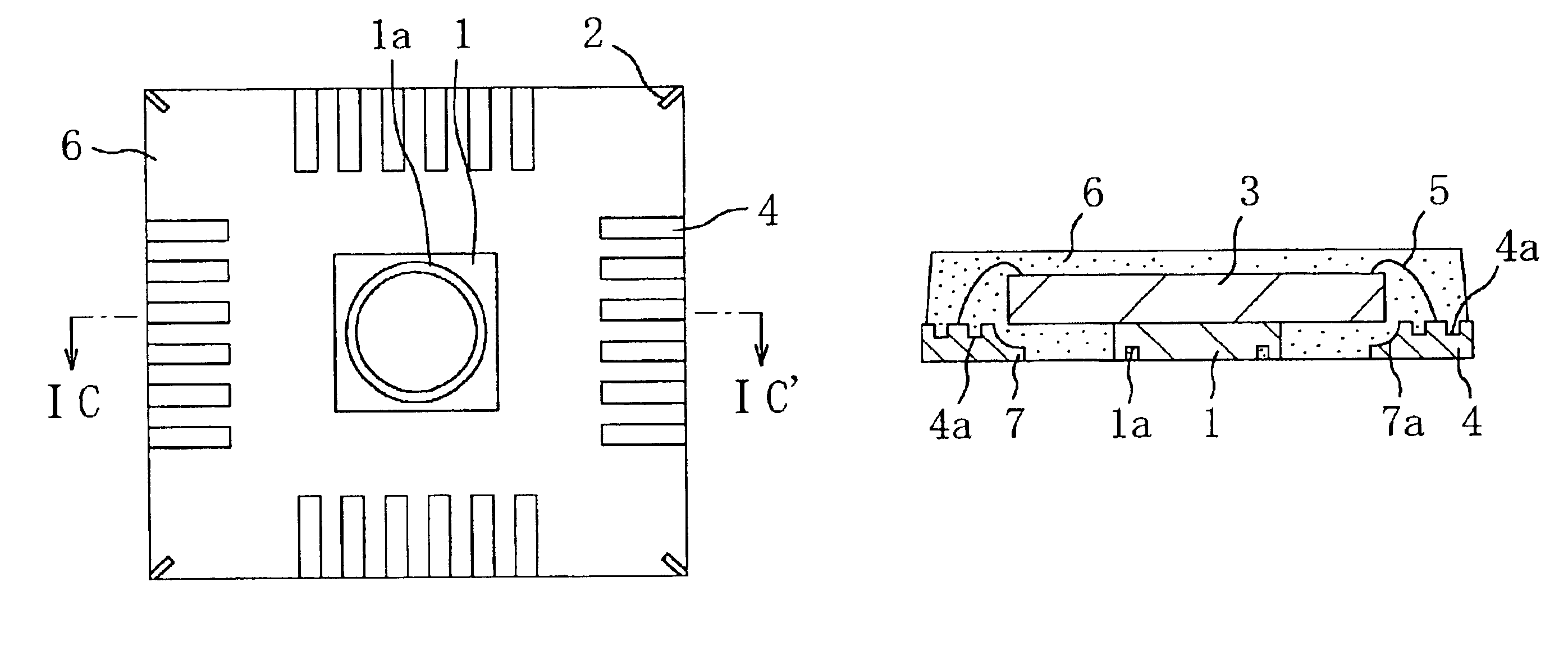
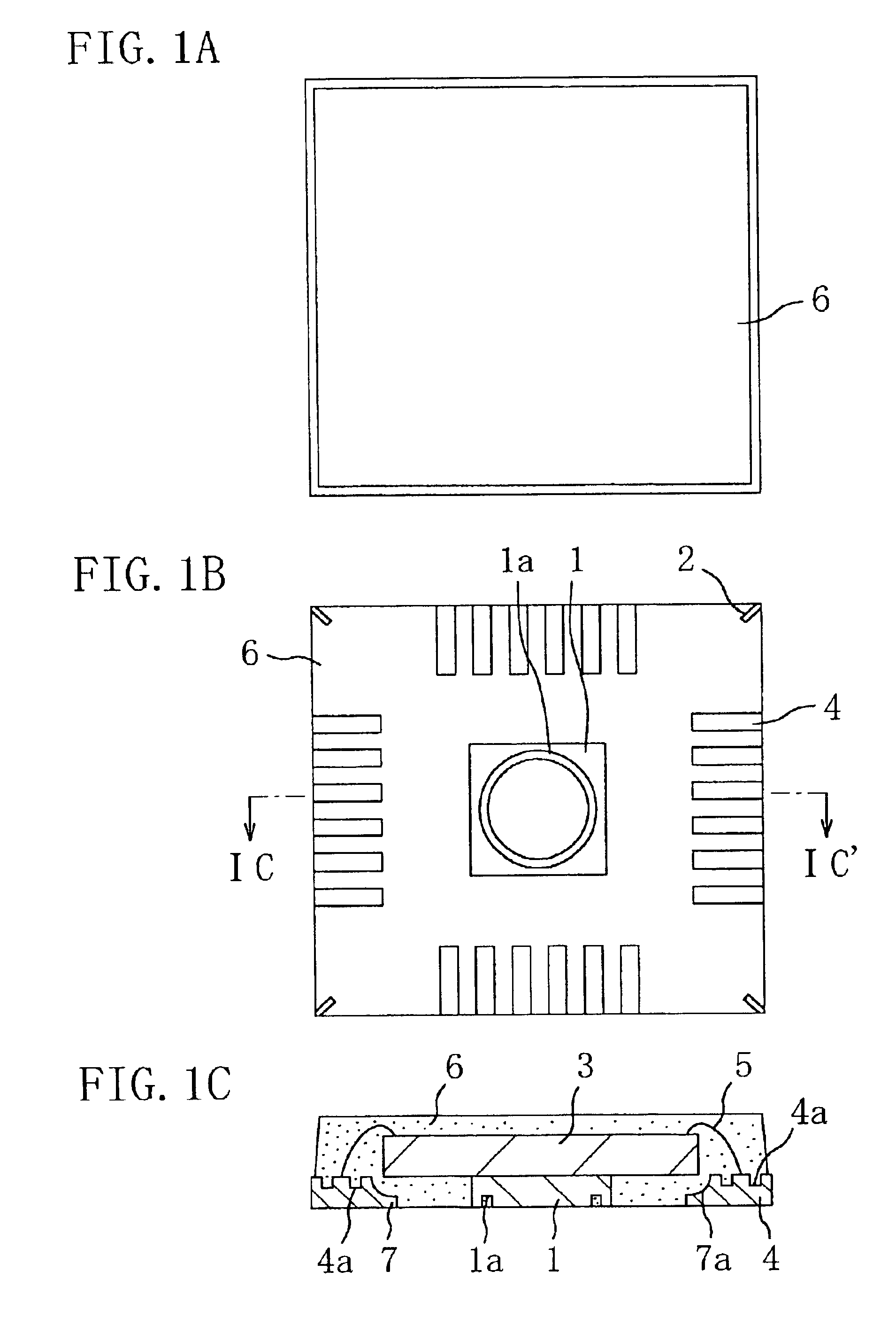
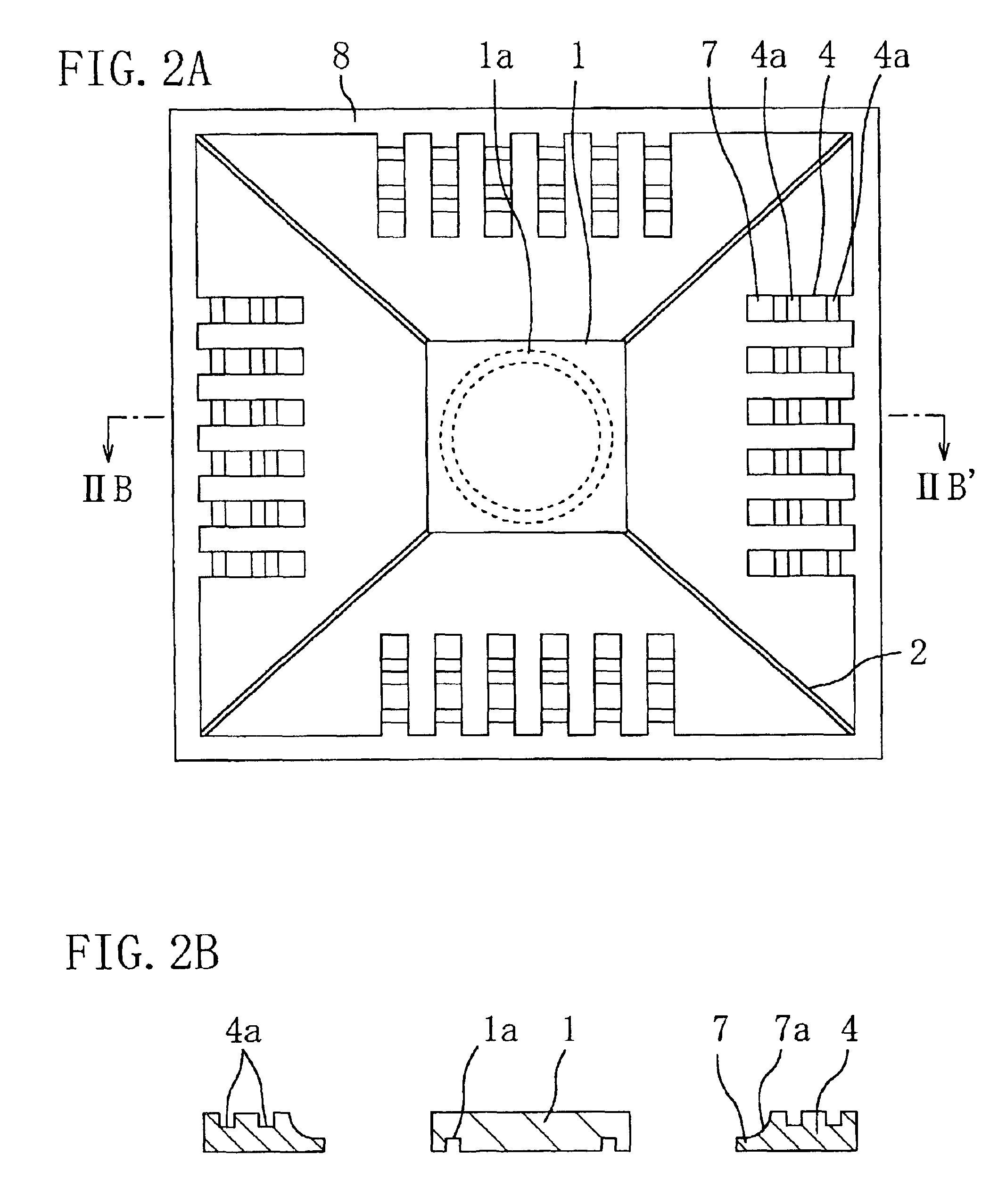
[0053]FIGS. 1A through IC schematically show a resin-encapsulation semiconductor device according to one embodiment of the invention. FIG. 1A is a plan view of the resin-encapsulation semiconductor device, FIG. 1B is a bottom view thereof and FIG. 1C is a cross-sectional view thereof taken along line 1C-1C′ of FIG. 1B.

[0054]The resin-encapsulation semiconductor device of this embodiment, which uses a lead frame, principally aims at realizing a CSP by increasing a ratio of the chip area to the package area.

[0055]As shown in FIGS. 1A through 1C, the resin-encapsulation semiconductor device of this embodiment includes a die pad 1 for mounting a semiconductor element, a plurality of supporting leads 2 for supporting the die pad 1 at its respective corners, a semiconductor element 3 mou...


PUM


Abstract

A resin-encapsulation semiconductor device of this invention includes a die pad for mounting a semiconductor element; a plurality of supporting leads; a semiconductor element; a plurality of leads disposed to have tips thereof opposing the die pad; metal wires; and an encapsulation resin for encapsulating the die pad excluding a bottom thereof, the leads excluding bottoms and outside edges thereof, connecting regions with the metal wires, the supporting leads and the semiconductor element. The outside edges of the leads are disposed on substantially the same plane as the side face of the encapsulation resin, and the tip of each lead has a thin portion where the thickness is reduced in an upper face thereof.

Description

BACKGROUND OF THE INVENTION[0001]The present invention relates to a resin-encapsulation semiconductor device using a lead frame and a method for fabricating the same. More particularly, it relates to a resin-encapsulation semiconductor device in which a die pad for mounting a semiconductor element is exposed from an encapsulation resin and a method for fabricating the same, and furthermore, it relates to a thin and highly reliable resin-encapsulation semiconductor device in which a semiconductor element with a large package area ratio can be packaged and a method for fabricating the same.[0002]Recently, in order to cope with downsizing of electronic equipment, semiconductor components such as a resin-encapsulation semiconductor device are required to have a high packaging density. Also in accordance with the downsizing, the semiconductor components have become small and thin. Furthermore, the semiconductor components are required to have a multi-pin structure in spite of their compa...

Claims


Application Information

Patent Timeline
Patent Type & Authority Patents(United States)
IPC IPC(8): H01L23/495H01L23/28H01L23/31H01L23/48H01L23/50
CPCH01L23/3107H01L23/49548H01L24/97H01L23/49503H01L2924/01033H01L2224/32014H01L2224/48091H01L2224/48247H01L2224/97H01L2924/01004H01L2924/01029H01L2924/01047H01L2924/01082H01L2924/01006H01L2924/01005H01L24/48H01L2224/85H01L2924/00014H01L2224/451H01L2924/181H01L24/45H01L2224/32055H01L2224/83385H01L2924/00015H01L2224/05599H01L2924/00012
Inventor MINAMIO, MASANORINOMURA, TORU
Owner TESSERA ADVANCED TECH
Features
  • R&D
  • Intellectual Property
  • Life Sciences
  • Materials
  • Tech Scout
  • Unparalleled Data Quality
  • Higher Quality Content
  • 60% Fewer Hallucinations
Learn More