Thin film capacitor and fabrication method thereof

Active Publication Date: 2005-06-21
DONGBU ELECTRONICS CO LTD +1
View PDF8 Cites 17 Cited by
  • Summary
  • Abstract
  • Description
  • Claims
  • Application Information

AI Technical Summary

Benefits of technology

[0015]In considerations of the above problems, it is an object of the present invention to enabl

Problems solved by technology

However, as a size of device becomes reduced due to high integration of semiconductor devices, an area of the upper metal wire becomes smaller.
However, with the methods for increasing the coupling ratio, there is a limit to reduction of the upper metal wire while maintaining the electrostatic capacity.

Method used


Image

  • Thin film capacitor and fabrication method thereof
  • Thin film capacitor and fabrication method thereof
  • Thin film capacitor and fabrication method thereof

Examples


third embodiment

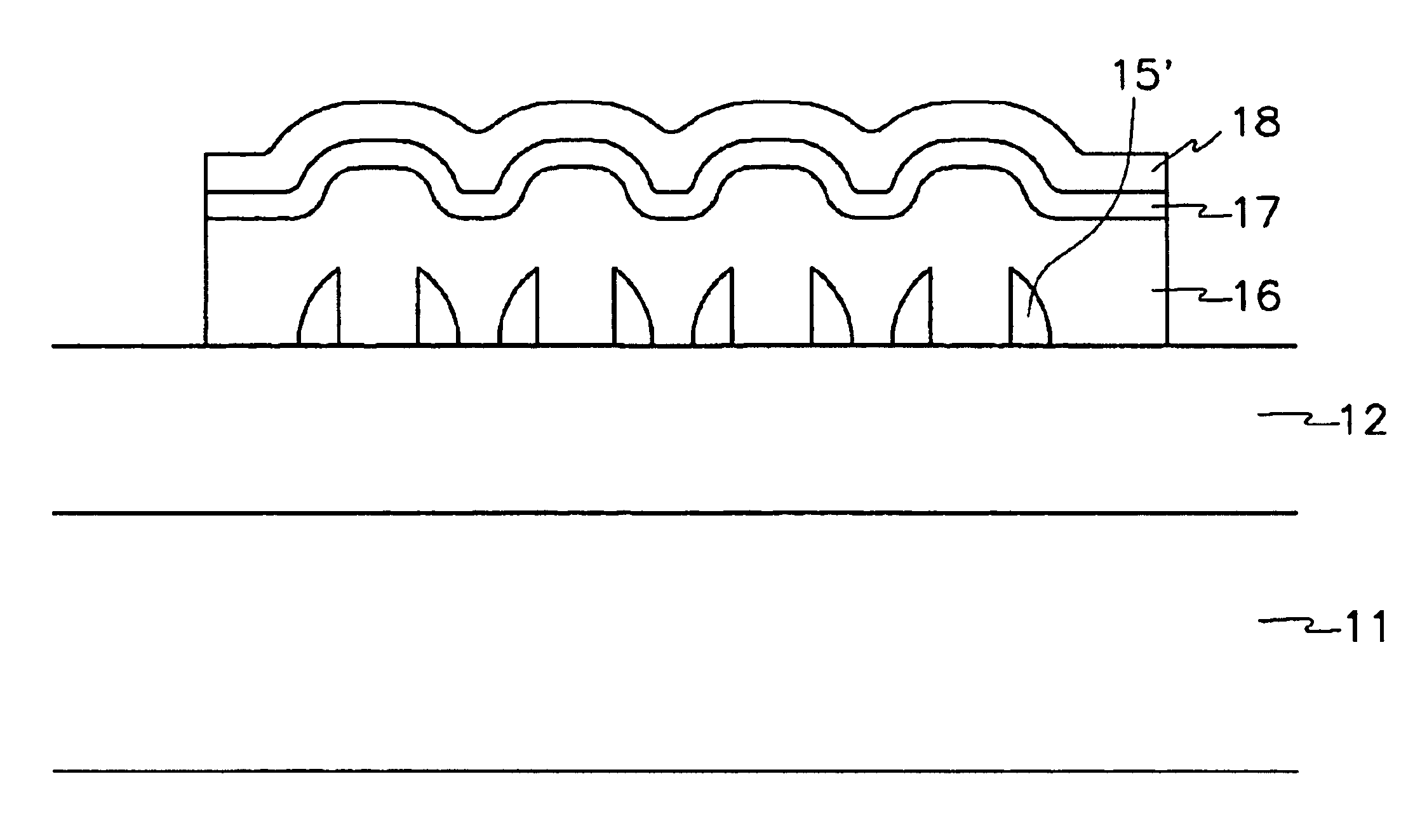
[0047]Namely, as shown in FIG. 4f, according to the present invention, the side wall 15′ is formed on the side surface of the projection 13′, here, the projection 13′ can be made of metal material or an oxide and the side wall 15′ can be made of a nitride.

[0048]The first electrode layer 16, the dielectric layer 17 and the second electrode layer 18 are formed at a predetermined width on the lower insulation film 12 including the projection 13′ and the side wall 15′. At this time, a projecting part exists on the surfaces of the first electrode layer 16, the dielectric layer 17 and the second electrode layer 18 due to the projection 13′ and the side wall 15′.

fourth embodiment

[0049]In addition, as shown in FIG. 5f, according to the present invention, the side wall 15′ is formed to be projected from the surface of the lower insulation film 12. This side wall 15′ is formed on the side surface of the projection 13′, and then is left after the projection 13′ is removed. In this case, the side wall 15′ can be formed of an oxide film.

[0050]The first electrode 16, the dielectric layer 17 and the second electrode layer 18 are formed at a predetermined width on the lower insulation film 12 including the side wall 15′. At this time, a projecting part exists on surfaces of the first electrode layer 16, the dielectric layer 17 and the second electrode layer 18 due to the side wall 15′. Thus, the side wall 15′ in the fourth embodiment of the present invention plays the same role as the projection in the first embodiment of the present invention.

[0051]Now, a method for fabricating the thin film capacitor of the present invention as described above will be in detail de...

first embodiment

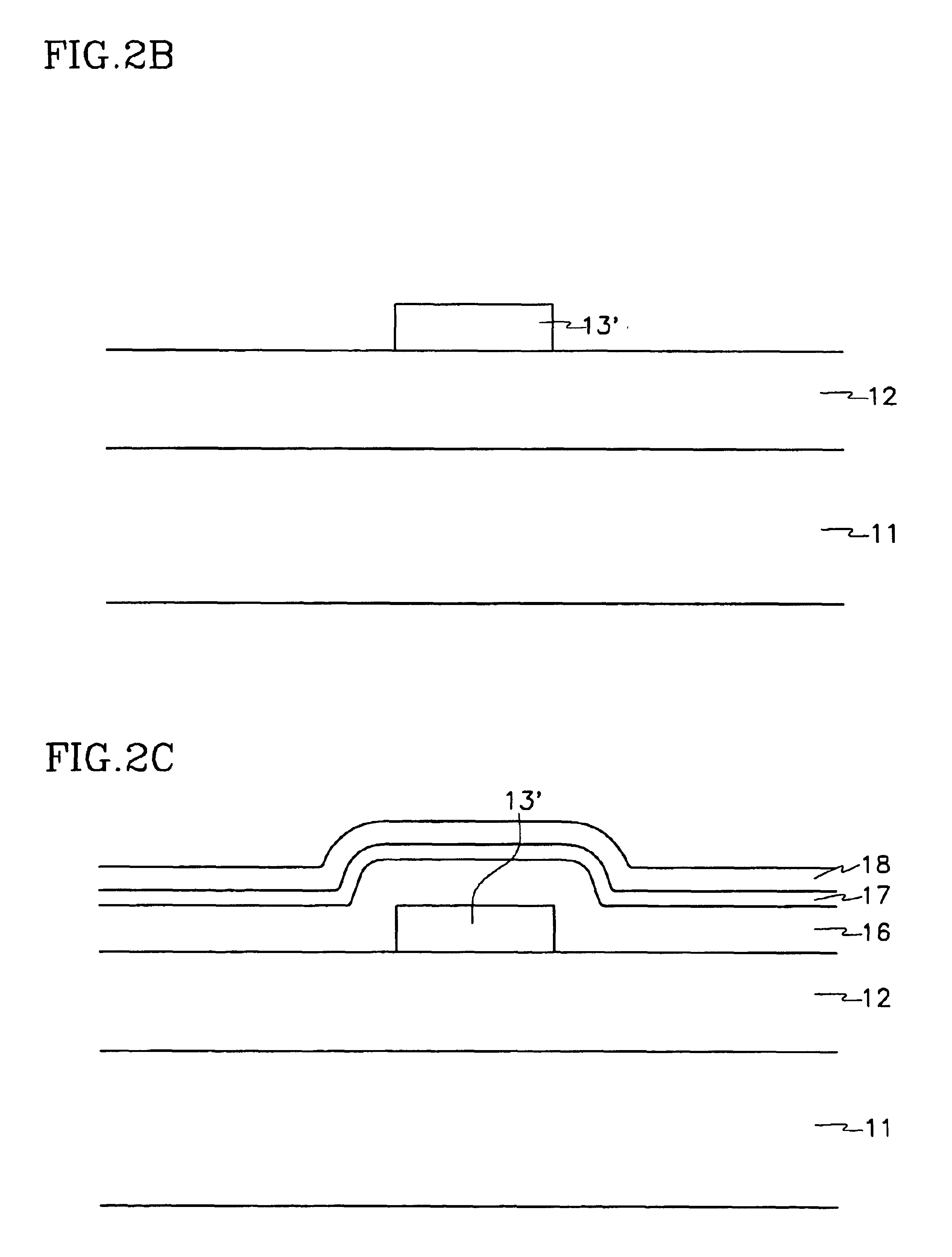
[0052]FIGS. 2a to 2d are sectional views showing a method for fabricating a thin film capacitor according to the present invention.

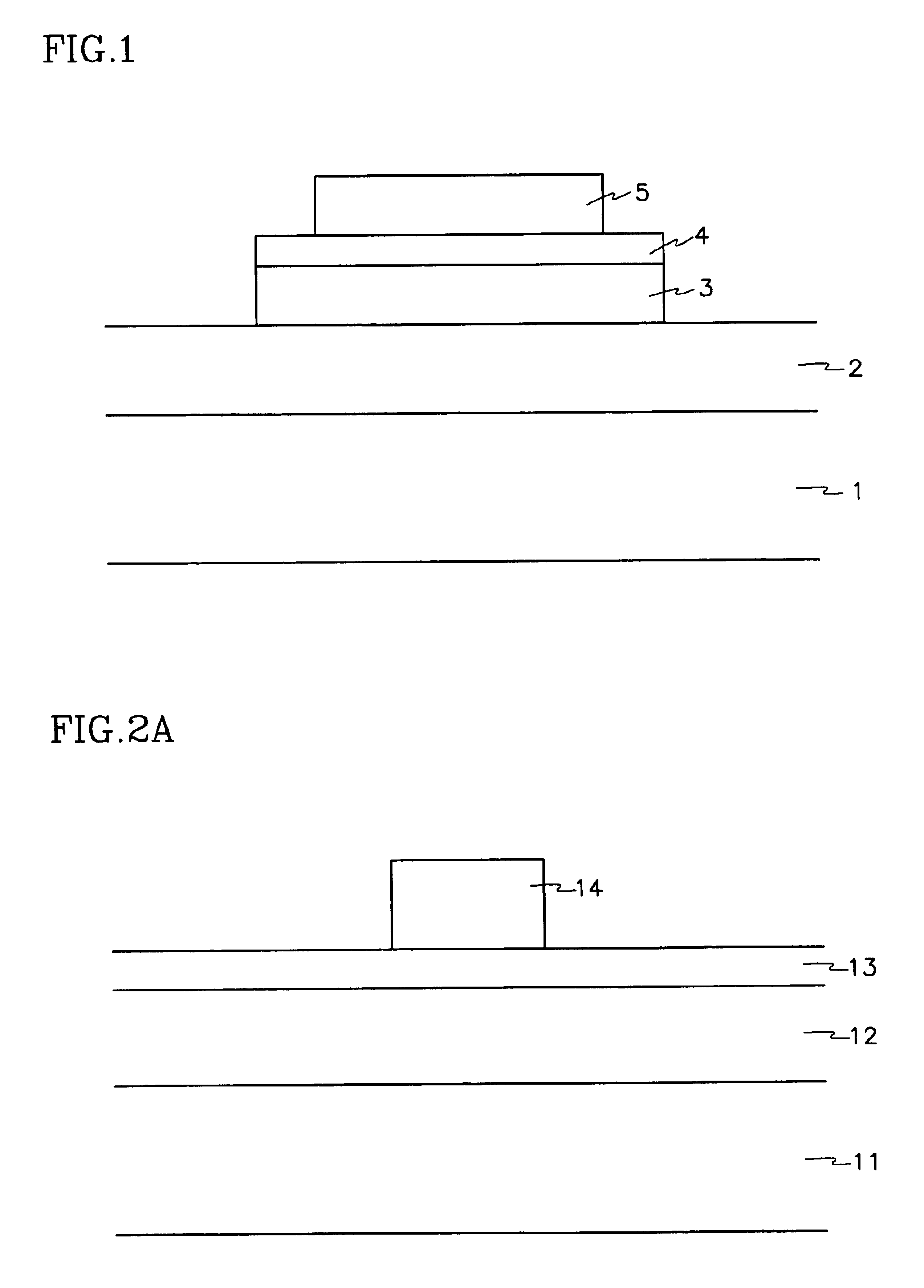
[0053]First, as shown in FIG. 2a, typical processes for fabricating a semiconductor device are first performed on a semiconductor substrate in order to form a structure 11 of the semiconductor substrate in which individual elements are formed, a lower insulation film 12 composed of an oxide film such as PSG is formed on the structure 11 of the semiconductor substrate, and then the lower insulation film 12 is planarized by using a chemical and mechanical polishing process.

[0054]Subsequently, a heterogeneous film 13 is formed on the planarized lower insulation film 12, and then a photosensitive film is applied, exposed and developed on the heterogeneous film 13 such that a photosensitive film pattern 14 to cover the lower insulation film 12, located under a region to be formed with a capacitor, by a predetermined width is formed.

[0055]At this time, the het...


PUM


Abstract

The present invention is directed to a method for fabricating a thin film capacitor of a metal / insulator / metal (MIM) structure, which is capable of enabling small-sizing of a semiconductor device while maintaining electrostatic capacity of a capacitor. The method comprises the steps of: forming a heterogeneous film on a lower insulation film on a structure of a semiconductor substrate; forming a plurality of projections by selectively etching the heterogeneous film; and forming a first electrode layer, a dielectric layer, and a second electrode layer on the lower insulation including the plurality of projections in order along a surface shape of the projections such that a plurality of projecting parts are formed in the first electrode layer, the dielectric layer and the second electrode layer, respectively.

Description

BACKGROUND OF THE INVENTION[0001](a) Field of the Invention[0002]The present invention relates to a fabrication method of a semiconductor device, and more particularly to a method for fabricating a thin film capacitor of a metal / insulator / metal (MIM) structure.[0003](b) Description of the Related Art[0004]Recently, in the field of analog circuit requiring a high speed operation, semiconductor devices for realizing high capacitance have been developed. In general, since an upper electrode and a lower electrode of a capacitor are made of a conductive polysilicon in a case where the capacitor has a PIP structure where a polysilicon, an insulator, and a polysilicon are stacked in order, a natural oxide film is formed by an oxidation reaction at an interface between the upper and lower electrodes and a dielectric film, which results in reduction of the total capacitance.[0005]To overcome this problem, the structure of capacitor has been changed to a metal / insulator / silicon (MIS) structur...

Claims


Application Information

Patent Timeline
IPC IPC(8): H01G4/005H01G4/012H01G4/228H01G4/33H01L21/02H01L23/522H01L27/01
CPCH01G4/005H01G4/33H01L23/5223H01L27/016H01L28/82H01L2924/0002H01L2924/00
Inventor SEO, YOUNG-HUN
Owner DONGBU ELECTRONICS CO LTD
Why Eureka
Try Eureka