

Compositions for thin-film capacitive device, high-dielectric constant insulating film, thin-film capacitance device, and thin-film multilayer ceramic capacitor
- Summary
- Abstract
- Description
- Claims
- Application Information
AI Technical Summary
Benefits of technology
Problems solved by technology
Method used
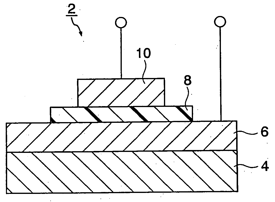
Image

Examples
example 2
[0093] Except for forming about 35 nm film thickness of NBT thin-film (dielectric thin-film) on the surface of CaRuO.sub.3 lower electrode thin-film, in the same way as example 1, surface roughness (Ra) of NBT thin-film and also electric characteristic (dielectric constant, tan .delta., the loss Q value, leak current and break-down voltage) and temperature characteristic of dielectric constant for the thin-film capacitor sample were evaluated. The result is shown in table 2. Further, the break-down voltage (Unit is kV / cm) was measured by increasing the voltage when measuring leak characteristic.
example 3
[0094] Except for forming about 50 nm film thickness of NBT thin-film (dielectric thin-film) on the surface of CaRuO.sub.3 lower electrode thin-film, in the same way as example 1, surface roughness (Ra) of NBT thin-film and also electric characteristic and temperature characteristic of dielectric constant for the thin-film capacitor sample were evaluated. The result is shown in table 2.
example 4
[0095] Except for forming about 100 nm film thickness of NBT thin-film (dielectric thin-film) on the surface of CaRuO.sub.3 lower electrode thin-film, in the same way as example 1, surface roughness (Ra) of NBT thin-film and also electric characteristic and temperature characteristic of dielectric constant for the thin-film capacitor sample were evaluated. The result is shown in table 2.
2TABLE 2 Film Surface Break-down Thickness Roughness Leak Current Voltage Dielectric Temperature The Loss Q (nm) Ra (nm) (A / cm.sup.2) (kV / cm) Constant Coefficient(ppm / .degree. C.) tan .delta. Value Ex. 2 35 0.6 5 .times. 10.sup.-7 >1000 150 +30 25 Ex. 3 50 0.6 1 .times. 10.sup.-7 >1000 150 +30 50 Ex. 4 100 0.6 4 .times. 10.sup.-8 >1000 150 +30 100
[0096] As shown in Table 2, when film thickness for c-axis orientation film was made thinner, it was confirmed that although leak property became little inferior, surface roughness and dielectric constant did not change.
[0097] Further, Reference 1 (Y. Sakash...
PUM
| Property | Measurement | Unit |
|---|---|---|
| Fraction | aaaaa | aaaaa |
| Thickness | aaaaa | aaaaa |
| Angle | aaaaa | aaaaa |
Abstract
Description
Claims
Application Information