
Method for plating electrodes of ceramic chip electronic components

a technology of electronic components and ceramic chips, applied in the direction of electrolysis components, basic electric elements, semiconductor devices, etc., can solve the problems of increasing the cost of forming electrodes. achieve excellent solder wettability

Inactive Publication Date: 2005-06-28
MURATA MFG CO LTD
View PDF11 Cites 10 Cited by
  • Summary
  • Abstract
  • Description
  • Claims
  • Application Information

AI Technical Summary

Benefits of technology

The present invention provides a method for plating electrodes of ceramic chip electronic components using tin (II) sulfamate as a tin salt, a complexing agent, and a brightener. The method limits the adhesion failure of the electrodes and provides a smooth plating film with excellent solder wettability. The plating bath also contains an antioxidant to prevent the oxidation of tin (II) ions and increase the lifetime of the plating bath. The concentration of the tin (II) sulfamate and the complexing agent are set within certain ranges to achieve a smooth plating film. The ceramic chip electronic components plated using this method do not show adhesion failure and have excellent solder wettability.

Problems solved by technology

However, the intrinsic physical properties of tin cause various problems in plating.
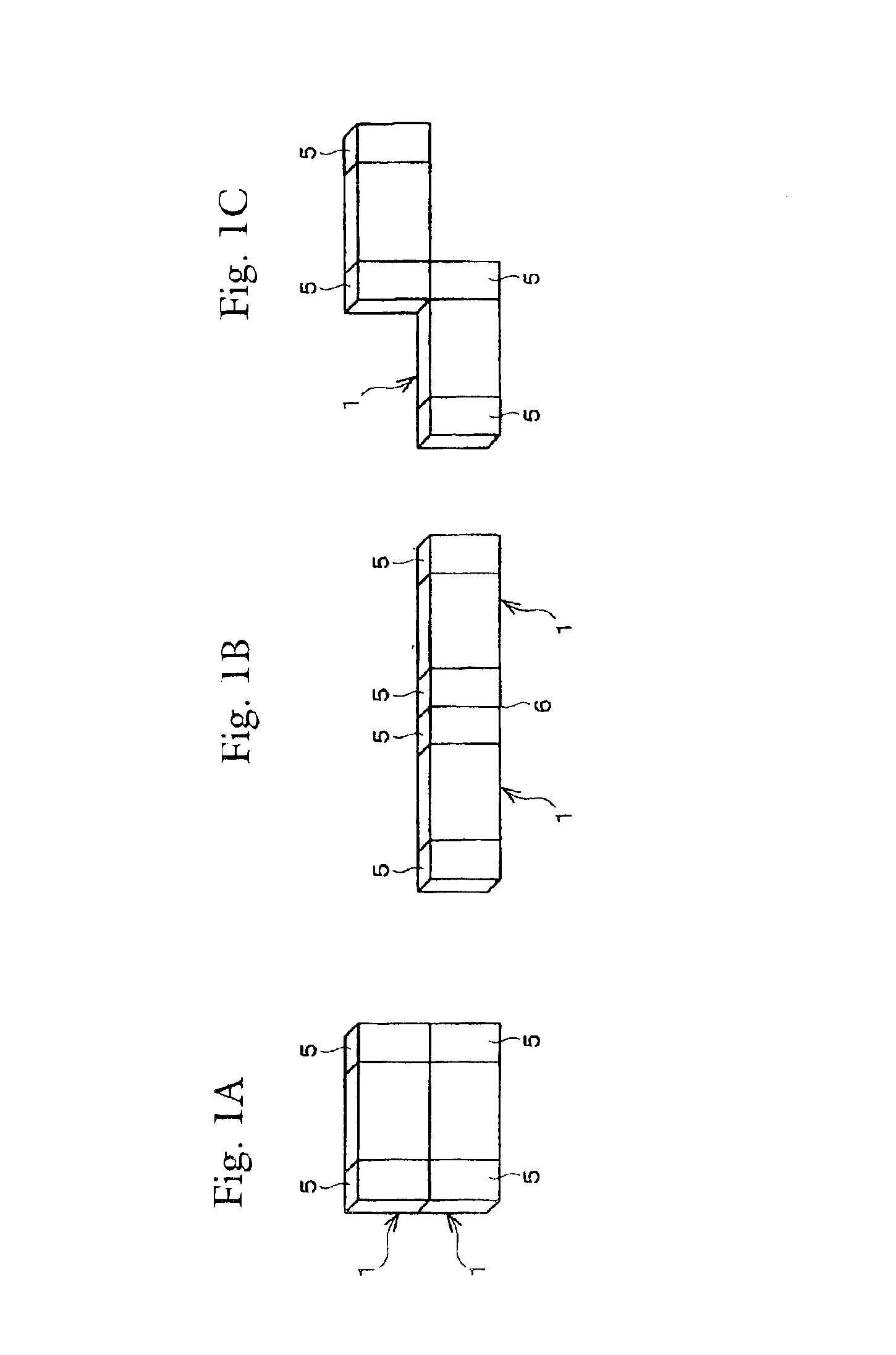
In particular, when ceramic chip electronic components (chips) containing ceramic and glass is subjected to tin plating, the chips are liable to adhere to one another.
This adhesion problem becomes particularly significant when the number of chips to be plated at a time is increased.
If the adhesion occurs, adhering chips themselves are defective.
In addition, some weakly adhering chips are likely to be separated during plating or drying.
The thickness of the plating films at the separated portions of these chips is very thin and, accordingly, these chips are defective.
Thus, defective chips are likely to be mixed among normal chips.
As chip components become smaller, it is expected that this adhesion problem will become more serious.

Method used


Image

  • Method for plating electrodes of ceramic chip electronic components
  • Method for plating electrodes of ceramic chip electronic components
  • Method for plating electrodes of ceramic chip electronic components

Examples


example 1

[0057]A method for plating electrodes of ceramic chip electronic components, according to the present invention, will now be concretely described with reference to the following examples and comparative examples.

[0058]Table 1 shows the compositions of plating baths used in Examples 1-1 to 1-5 and the evaluation results of the plating films formed in these plating baths.

[0059]

TABLE 1Plating bathEvaluationComplexingConductingAdhesionHull cellExampleTin saltagentagentBrightenerAntioxidantpHratiotest1-1Tin (II)DiammoniumSodiumDimethylalkylPyrocatechol3.5goodgoodsulfamatehydrogensulfamatelauryl betaine1.0 g / L(7%)0.20 mol / Lcitrate1.00 mol / L0.3 g / L1.50 mol / L1-2Tin (II)Malonic acidSodiumβ-naphtholHydroquinone4.0goodverysulfamate1.20 mol / Lsulfamateethoxylate1.0 g / L(5%)good0.40 mol / L1.00 mol / L0.1 g / L1-3Tin (II)HeptoicSodiumPolyoxyethyleneAscorbic acid5.0goodverysulfamateacidsulfamateoctylphenyl1.0 g / L(6%)good0.10 mol / L1.00 mol / L2.00 mol / Lether 0.5 g / L1-4Tin (II)GluconicSulfamicPhenolsulfonicA...

example 2

[0074]In order to obtain a lustrous plating film, the kinds of the brightener were varied and evaluated according to the above-described criteria. Since it has already been known that the compositions in Table 1 lead to preferred results, the brightener evaluation was performed based on Example 1-1. Specifically, the brightener of Example 1-1 was replaced with the brighteners of Examples 2-1 to 2-5 shown in Table 3 to prepare the plating baths of Examples 2-1 to 2-5. The pH was set at 5.

[0075]

TABLE 3Plating bathEvaluationComplexingConductingAdhesionHullExampleTin saltagentagentBrightenerAntioxidantpHratiocell test2-1Tin (II)DiammoniumSodiumPolyoxyethylenePyrocatechol5.0Goodgoodsulfamatehydrogensulfamatealkylpropylenediamine1.0 g / L(4%)0.20citrate1.00 mol / L0.3 g / L2-2mol / L1.50 mol / Lα-naphthol ethoxylateGoodvery0.1 g / L(6%)good2-3PolyoxyethyleneGoodverynonylphenyl ether(7%)good0.3 g / L2-4α-naphthol ethoxylateGoodgood0.3 g / L(3%)2-5PolyoxyethyleneGoodgooddodecylamine(5%)0.3 g / L

[0076]Table 3...


PUM

PropertyMeasurementUnit
concentrationaaaaaaaaaa
sizeaaaaaaaaaa
concentrationaaaaaaaaaa

Abstract

A method for plating electrodes of ceramic chip electronic components includes performing electroplating in a plating bath. The plating bath contains tin (II) sulfamate, acting as a tin (II) salt; a complexing agent including at least one selected from the group consisting of citric acid, gluconic acid, pyrophosphoric acid, heptoic acid, malonic acid, malic acid, salts of these acids, and gluconic lactone; and a brightener including at least one surfactant having an HLB value of about 10 or more. The tin plating adhesion of the resulting ceramic chip electronic components can be limited to a certain level.

Description

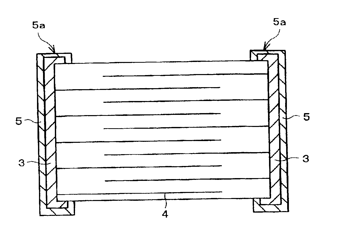
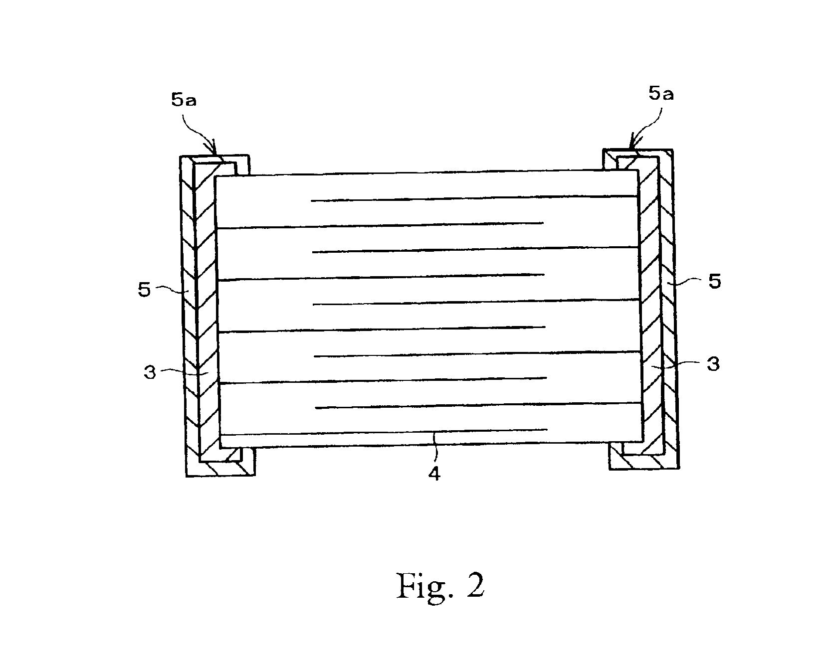
BACKGROUND OF THE INVENTION[0001]1. Field of the Invention[0002]The present invention relates to methods for forming electrodes of ceramic chip electronic components. In particular, the present invention relates to a method for plating electrodes of ceramic chip electronic components and to a ceramic chip electronic component having electrodes plated by the method.[0003]2. Description of the Related Art[0004]Electrodes of electronic components formed of ceramics, glass, plastics and the like, are generally plated with a tin-lead alloy in order to improve the solder wettability thereof. Tin has been replacing the tin-lead alloy used to plate the electrodes as the desire for lead-free plating has intensified. However, the intrinsic physical properties of tin cause various problems in plating.[0005]In particular, when ceramic chip electronic components (chips) containing ceramic and glass is subjected to tin plating, the chips are liable to adhere to one another. This adhesion is cause...

Claims


Application Information

Patent Timeline
Patent Type & Authority Patents(United States)
IPC IPC(8): C25D3/32C25D7/00C25D7/12C25D17/16
CPCC25D3/32C25D17/16C25D7/00
Inventor MOTOKI, AKIHIROHIGUCHI, SHOICHITAKANO, YOSHIHIKOHAMADA, KUNIHIKO
Owner MURATA MFG CO LTD
Learn More