Method for depositing thin film using plasma chemical vapor deposition

a chemical vapor deposition and thin film technology, applied in the field of thin film deposition process, can solve the problems of large amount of charges and non-uniform thickness of the depositing thin film, and achieve the effect of improving chemical vapor deposition

Inactive Publication Date: 2005-06-28
INNOLUX CORP
View PDF2 Cites 8 Cited by
  • Summary
  • Abstract
  • Description
  • Claims
  • Application Information

AI Technical Summary

Benefits of technology

[0007]Accordingly, the present invention provides a method for depositing thin film using plasma enhanced ch...

Problems solved by technology

However, as the thin film that is being deposited on the substrate is an insulating material layer or a high resistance thin film, such as, intrinsic amorphous silicon, a large quantity of charges is accumulated on the surface of the electrod...

Method used


Image

  • Method for depositing thin film using plasma chemical vapor deposition
  • Method for depositing thin film using plasma chemical vapor deposition

Examples


Embodiment Construction

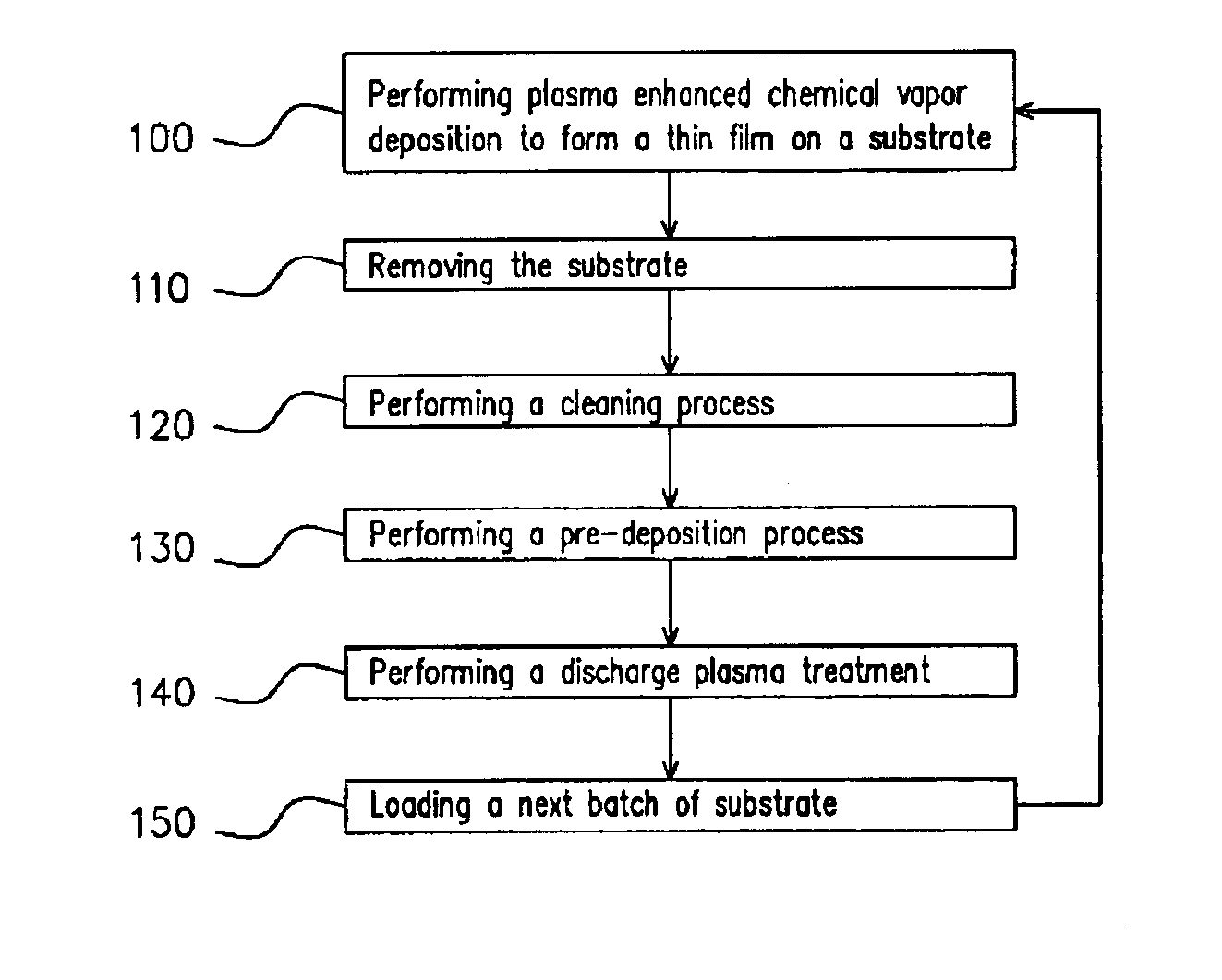
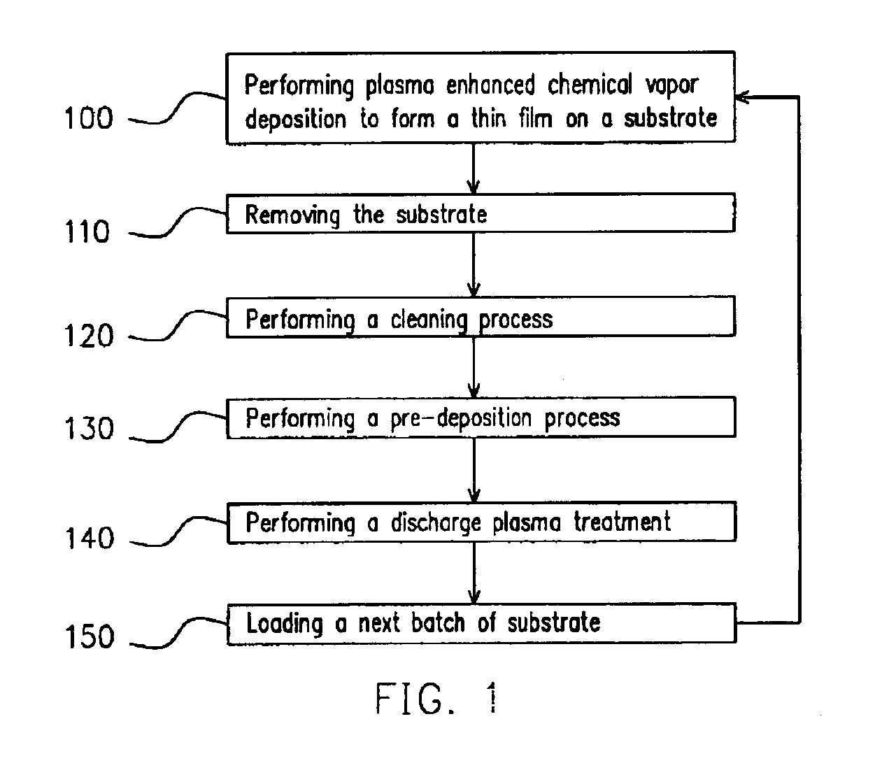
[0015]The present invention employs plasma enhanced chemical vapor deposition to deposit a thin film. Particularly, a discharge plasma treatment is performed after the pre-deposition process is conducted. The amount of the accumulated charges on the electrode surface in the chamber is greatly reduced to minimize the effects of the accumulated charges. The uniformity of the thickness of the thin film is thereby improved. The present invention is generally applicable in semiconductor processing, as illustrated in the following embodiment.

[0016]FIG. 1 is a flow diagram illustrating a method of thin film deposition using plasma enhanced chemical vapor deposition according to an embodiment of the present invention.

[0017]Referring to FIG. 1, in step 100, a plasma enhanced chemical vapor deposition process is performed to form a thin film on a substrate. Chemical reaction is enhanced by plasma to form a layer of thin film on the substrate that is placed in the PECVD chamber.

[0018]Thereafte...


PUM

PropertyMeasurementUnit
Electrical resistanceaaaaaaaaaa

Abstract

A thin film deposition method using plasma enhanced chemical vapor deposition is described. In a plasma enhanced chemical vapor deposition chamber, plasma is used to enhance the chemical reaction to form a thin film on a substrate. The substrate is then removed, followed by passing a cleaning gas into the chamber to remove residues in the chamber. Before loading another batch of substrate in the chamber, a pre-deposition process is performed to isolate contaminants generated from the cleaning process. A discharge plasma treatment is then conducted to lower the amount of accumulated electrical charges.

Description

BACKGROUND OF INVENTION[0001]1. Field of the Invention[0002]The present invention relates to a deposition process for a semiconductor device. More particularly, the present invention relates to a method for depositing thin film using plasma enhanced chemical vapor deposition.[0003]2. Description of Related Art[0004]Currently, chemical vapor deposition is the most important process in semiconductor manufacturing for depositing a thin film. In any semiconductor device where a thin film is required, whether the thin film is conductive, semi-conductive or dielectrics, the thin film is formed by chemical vapor deposition. Chemical vapor deposition is defined as the formation of a thin film by the reaction of vapor-phase chemicals that contain the required constituents. Thus, the thin film formed by such a method is superior in crystallinity, stoichiometry and other relevant material properties.[0005]To lower the required reaction temperature so as to reduce the thermal budget of the proc...

Claims


Application Information

Patent Timeline
IPC IPC(8): C23C16/44
CPCC23C16/4405C23C16/4404
Inventor LIN, FRANK
Owner INNOLUX CORP
Why Eureka
Try Eureka