Low stress sidewall spacer in integrated circuit technology

a technology of integrated circuits and sidewalls, applied in the field of silicon-based silicon devices, can solve the problems of affecting the performance of transistors, existing siliciding and saliciding have not succeeded in solving all the problems relating to connecting metal contacts to silicon, and the integration circuit is not suitable for all applications, so as to improve the performance of the integrated circuit, improve the electrical resistance, and improve the effect of chemical vapor deposition

Active Publication Date: 2005-07-14
INNOVATIVE FOUNDRY TECH LLC
View PDF10 Cites 5 Cited by
  • Summary
  • Abstract
  • Description
  • Claims
  • Application Information

AI Technical Summary

Benefits of technology

[0019] The present invention provides a method of forming an integrated circuit. A gate dielectric is formed on a semiconductor substrate, and a gate is formed on the gate dielectric. Source / drain junctions are formed in the semiconductor substrate. A sidewall spacer is formed around the gate using a low power plasma enhanced chemical vapor deposition (PECVD) process. A silicide is formed on the source / drain junctions and on the gate, and an interlayer dielectric is deposited above the semiconductor substrate. Contacts then are formed in the interlayer dielectric to the silicide. This method significantly lowers the electrical resistance between the contacts and the silicon or polysilicon greatly improving performance of the integrated circuit. The PECVD process preferably is performed within a low bias power range of about 100 watts to about 200 watts.

Problems solved by technology

Integrated circuits are made in and on silicon wafers by extremely complex systems that require the coordination of hundreds or even thousands of precisely controlled processes to produce a finished semiconductor wafer.
As transistors have decreased in size, it has been found that the electrical resistance between the metal contacts and the silicon substrate or the polysilicon has increased to the level where it negatively impacts the performance of the transistors.
However, existing siliciding and saliciding have not succeeded in solving all the problems related to connecting metal contacts to silicon.
The problems include, but are not limited to, encroachment by the silicide under the sidewall spacer adjacent the gate.
Piping of the silicide adversely affects the performance of the transistor.
Solutions to these problems have been long sought but prior developments have not taught or suggested any solutions and, thus, solutions to these problems have long eluded those skilled in the art.

Method used


Image

  • Low stress sidewall spacer in integrated circuit technology
  • Low stress sidewall spacer in integrated circuit technology
  • Low stress sidewall spacer in integrated circuit technology

Examples


Embodiment Construction

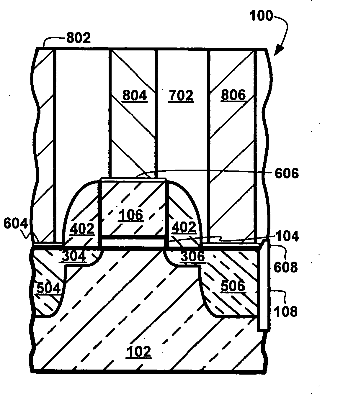
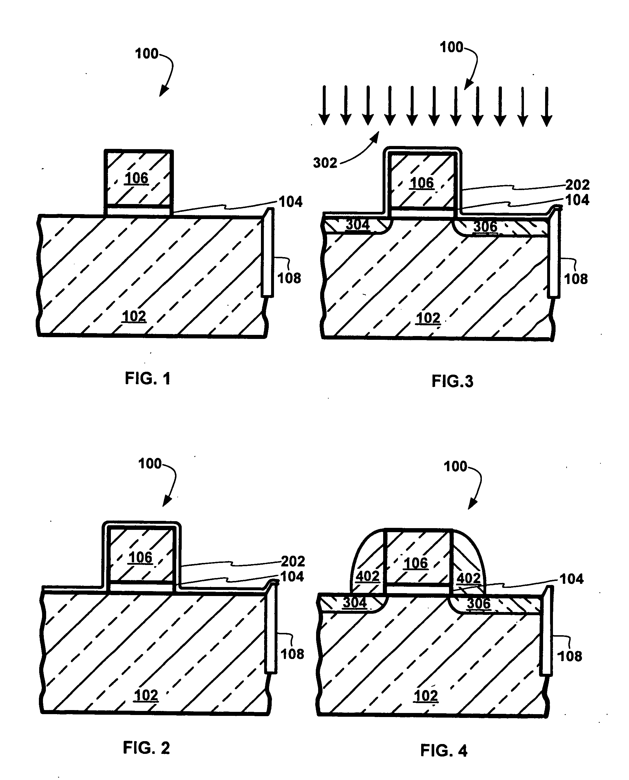
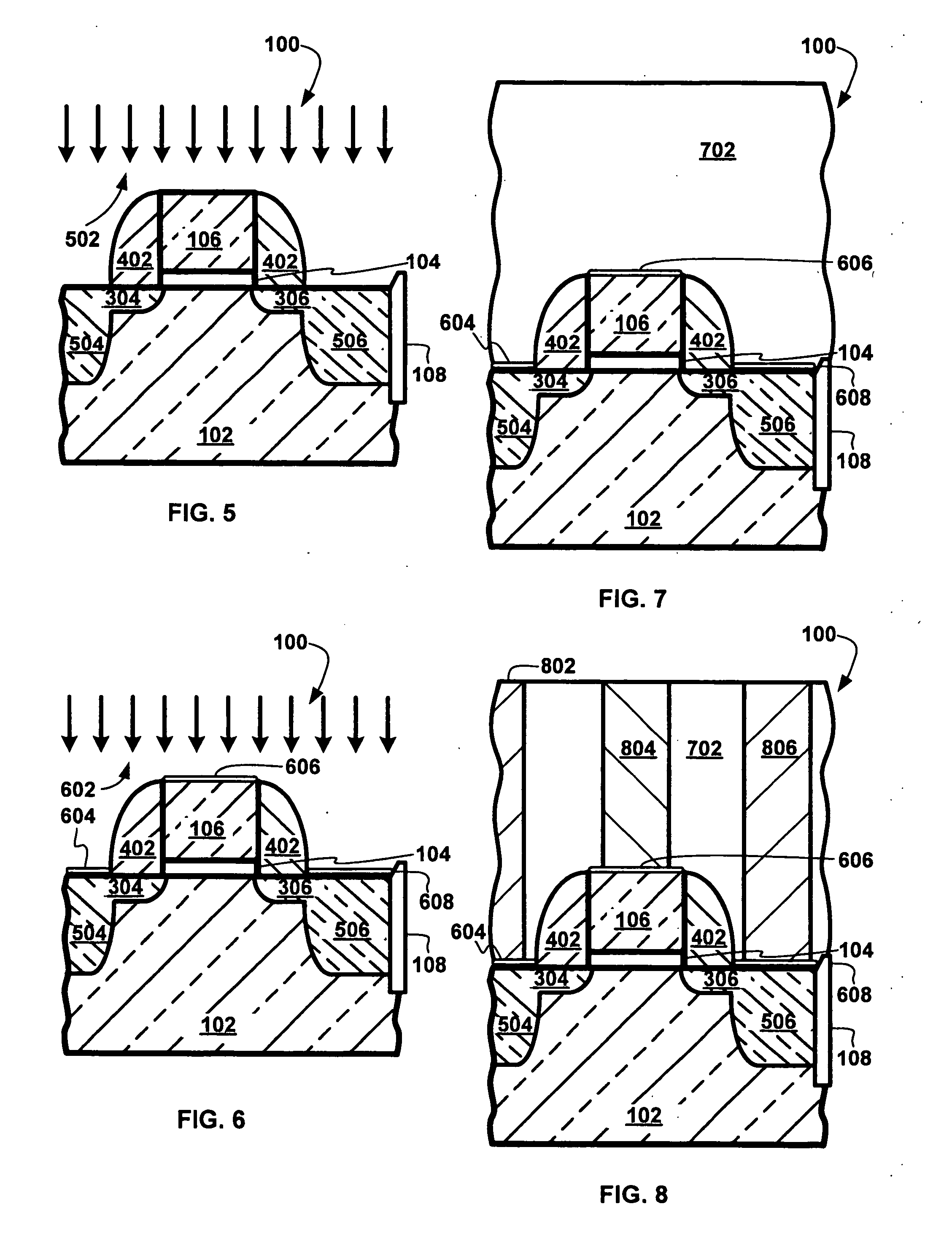
[0031] In the following description, numerous specific details are given to provide a thorough understanding of the invention. However, it will be apparent to one skilled in the art that the invention may be practiced without these specific details. In order to avoid obscuring the present invention, some well-known configurations and process steps are not disclosed in detail. In addition, the drawings showing embodiments of the apparatus are semi-diagrammatic and not to scale and, particularly, some of the dimensions are for the clarity of presentation and may be exaggerated in the drawing FIGs. The same numbers will be used in all the drawing FIGs. to relate to the same elements.

[0032] The term “horizontal” as used herein is defined as a plane parallel to a substrate or wafer. The term “vertical” refers to a direction perpendicular to the horizontal as just defined. Terms, such as “on”, “above”, “below”, “bottom”, “top”, “side” (as in “sidewall”), “higher”, “lower”, “over”, and “u...


PUM


Abstract

A method of forming an integrated circuit with a semiconductor substrate is provided. A gate dielectric is formed on the semiconductor substrate, and a gate is formed on the gate dielectric. Source/drain junctions are formed in the semiconductor substrate. A sidewall spacer is formed around the gate using a low power plasma enhanced chemical vapor deposition process A silicide is formed on the source/drain junctions and on the gate, and an interlayer dielectric is deposited above the semiconductor substrate. Contacts are then formed in the interlayer dielectric to the silicide.

Description

BACKGROUND [0001] 1. Technical Field [0002] The present invention relates generally to semiconductor technology, and more specifically to siliciding in semiconductor devices. [0003] 2. Background Art [0004] Electronic products are used in almost every aspect of life, and the heart of these electronic products is the integrated circuit. Integrated circuits are used in everything from airplanes and televisions to wristwatches. [0005] Integrated circuits are made in and on silicon wafers by extremely complex systems that require the coordination of hundreds or even thousands of precisely controlled processes to produce a finished semiconductor wafer. Each finished semiconductor wafer has hundreds to tens of thousands of integrated circuits, each worth hundreds or thousands of dollars. [0006] Integrated circuits are made up of hundreds to millions of individual components. One common component is the semiconductor transistor. The most common and important semiconductor technology presen...

Claims


Application Information

Patent Timeline
Patent Type & Authority Applications(United States)
IPC IPC(8): H01L21/336
CPCH01L29/6659H01L29/665H01L21/18H01L21/24
Inventor NGO, MINH VANCHAN, SIMON SIU-SINGBESSER, PAUL R.KING, PAUL L.RYAN, ERROL TODDCHIU, ROBERT J.
Owner INNOVATIVE FOUNDRY TECH LLC
Why Eureka
Try Eureka