Ferroelectric random access memory and methods of fabricating the same

a random access memory and ferroelectric technology, applied in the field of semiconductor devices, can solve the problems of oxidizing the conductive pattern of the interconnection line, increasing the cost of semiconductor fabrication, and performing more processing steps, and achieve the effect of enhancing chemical vapor deposition

Inactive Publication Date: 2008-04-17
SAMSUNG ELECTRONICS CO LTD
View PDF2 Cites 5 Cited by
  • Summary
  • Abstract
  • Description
  • Claims
  • Application Information

AI Technical Summary

Benefits of technology

[0014] The etch-stop layer may include an insulating material to prevent oxygen atoms from penetrating. The etch-stop layer may be formed using at least one of low pressure chemical vapor deposition silicon nitride (LP-CVD SiN), plasma enhanced chemical vapor deposition silicon nitride (PE-CVD SiN), chemical vapor deposition aluminum oxide (CVD Al2O3), and atomic layer deposition aluminum oxide (ALD Al2O3). The etch-stop layer may be formed to cover the entire surface of the semiconductor substrate during the annealing, preventing oxygen atoms from coming in contact with the conductive pattern.

Problems solved by technology

In recent years, limitations of dynamic random access memories (DRAMs) related to volatility have led to research of a ferroelectric random access memory (FeRAM) having a ferroelectric thin film.
However, conductive patterns constituting interconnection lines may be oxidized by the oxygen annealing.
Performing more processing steps increases the semiconductor fabricating cost.

Method used


Image

  • Ferroelectric random access memory and methods of fabricating the same
  • Ferroelectric random access memory and methods of fabricating the same
  • Ferroelectric random access memory and methods of fabricating the same

Examples


Embodiment Construction

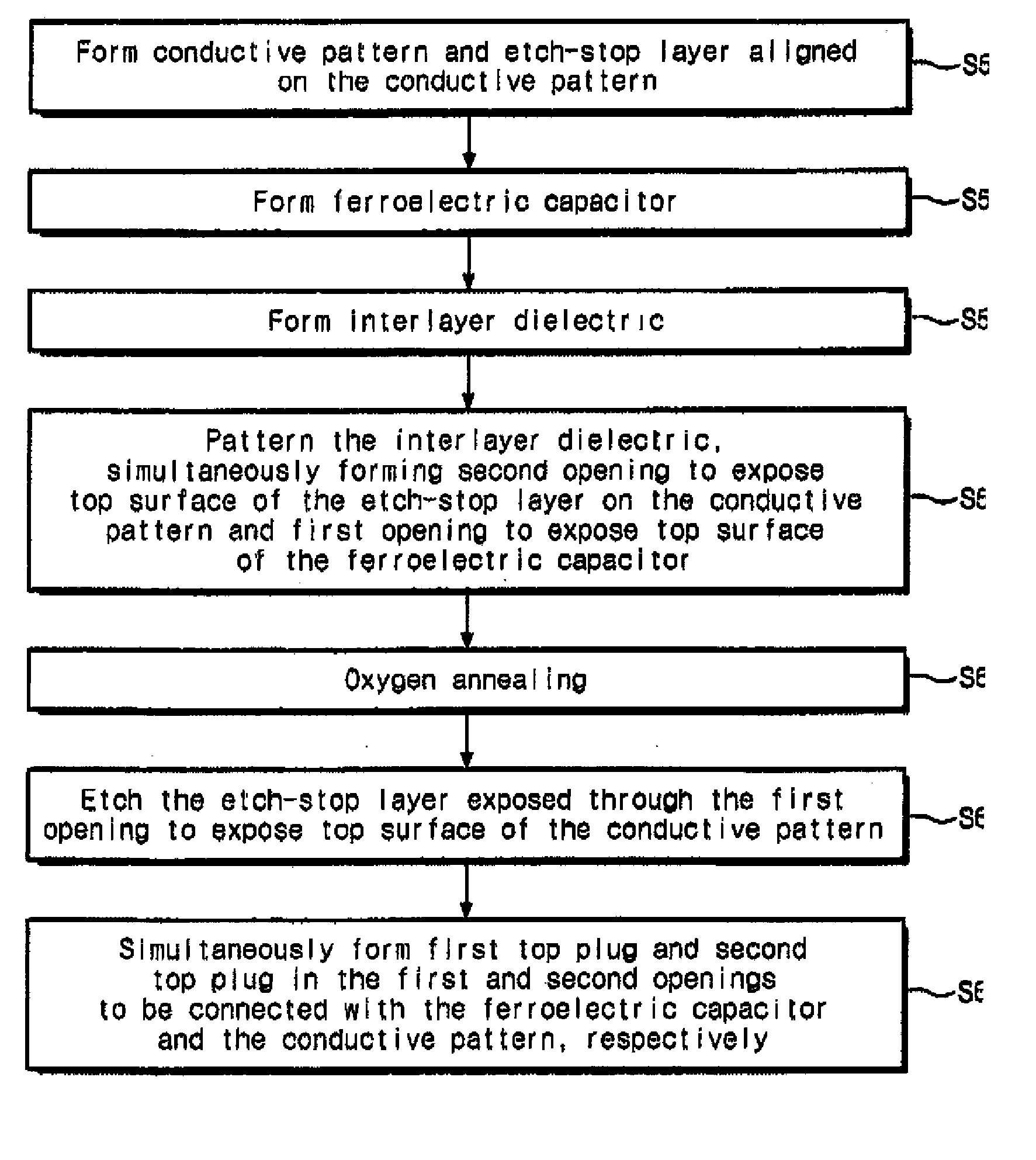
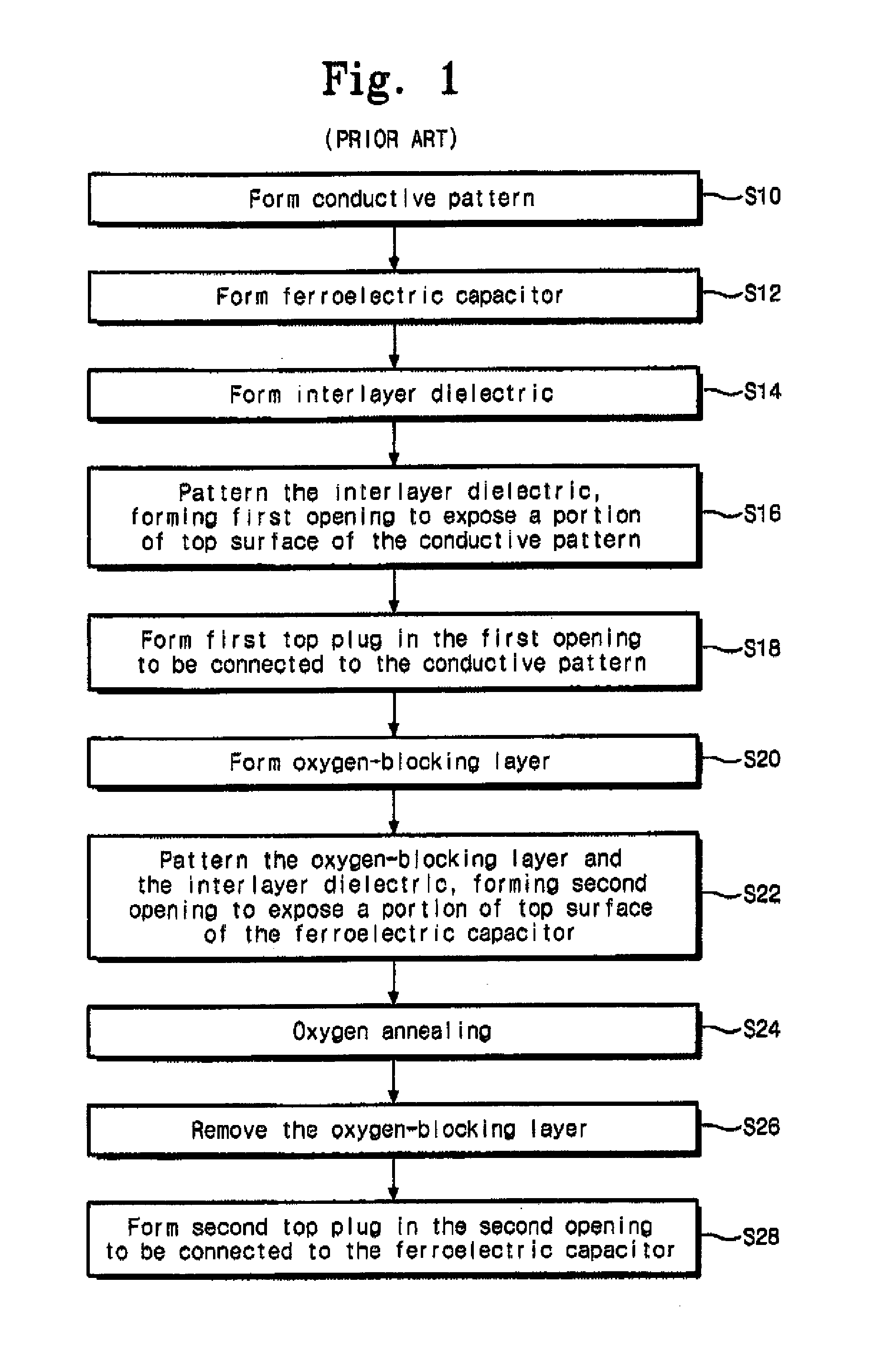
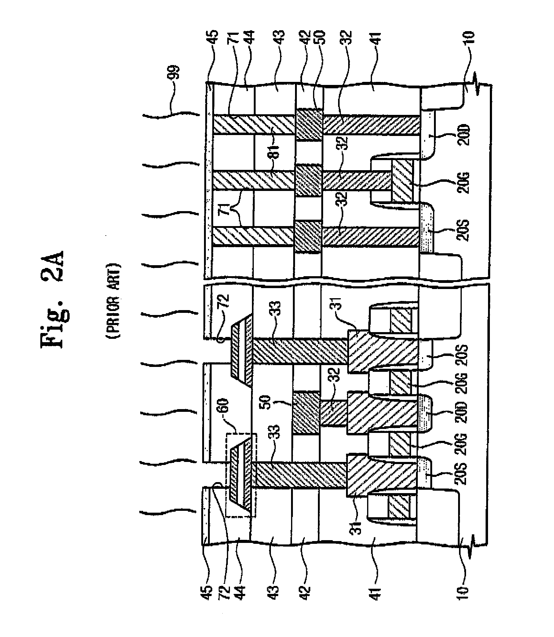
[0028] The present invention will now be described more fully with reference to the accompanying drawings, in which illustrative embodiments of the invention are shown. The invention, however, may be embodied in various different forms, and should not be construed as being limited only to the illustrated embodiments. Rather, these embodiments are provided as examples, to convey the concept of the invention to one skilled in the art. Accordingly, known processes, elements, and techniques are not described with respect to some of the embodiments of the present invention. Throughout the drawings and written description, like reference numerals will be used to refer to like or similar elements. Also, in the drawings, the thicknesses of layers and regions are exaggerated for clarity. It is also understood that when a layer is referred to as being “on” another layer or substrate, it can be directly on the other layer or substrate, or intervening layers may also be present.

[0029] A method...


PUM

PropertyMeasurementUnit
ferroelectricaaaaaaaaaa
conductiveaaaaaaaaaa
volatilityaaaaaaaaaa

Abstract

A method of forming a ferroelectric random access memory includes sequentially forming a conductive pattern, an etch-stop layer, a ferroelectric capacitor and an interlayer dielectric on a semiconductor substrate, which includes a first region and a second region. The ferroelectric capacitor is formed on the first region and the conductive pattern is formed on the second region. The interlayer dielectric is patterned to simultaneously form a first opening to expose a top surface of the ferroelectric capacitor and a second opening to expose a top surface of the etch-stop layer. The patterned interlayer dielectric is annealed in an ambient atmosphere, including oxygen atoms. The etch-stop layer exposed through the second opening is etched to expose a top surface of the conductive pattern. First and second top plugs are formed to connect to the ferroelectric capacitor and the conductive pattern through the first and second openings, respectively.

Description

CROSS-REFERENCE TO RELATED APPLICATION [0001] A claim of priority is made to Korean Patent Application No. 10-2006-0087664, filed on Sep. 11, 2006, the subject matter of which is hereby incorporated by reference. BACKGROUND [0002] 1. Field of the Invention [0003] The present invention relates to semiconductor devices and methods of fabricating the same. More specifically, the present invention is directed to a ferroelectric random access memory and methods of fabricating the ferroelectric random access memory. [0004] 2. Description of the Related Art [0005] In recent years, limitations of dynamic random access memories (DRAMs) related to volatility have led to research of a ferroelectric random access memory (FeRAM) having a ferroelectric thin film. The ferroelectric thin film exhibits hysterisis characteristics, which result from remnant polarization characteristics of ferroelectric materials. The FeRAM uses the hysterisis characteristics to retain its stored data irrespective of p...

Claims


Application Information

Patent Timeline
Patent Type & Authority Applications(United States)
IPC IPC(8): H01L21/8242H01L27/108
CPCH01L27/11502H01L28/57H01L27/11507H10B53/30H10B53/00H01L27/10H10B12/00
Inventor PARK, JUNG-HOONJOO, HEUNG-JIN
Owner SAMSUNG ELECTRONICS CO LTD
Why Eureka
Try Eureka