Group iii-v solar cell and method of manufacturing the same

a solar cell and solar cell technology, applied in the field of solar cells, can solve the problems of low photoelectric conversion efficiency, high price, and inaccessibility to ordinary households, and achieve the effects of enhancing chemical vapor deposition, and increasing the photoelectric conversion efficiency of solar cells

Inactive Publication Date: 2011-12-22
CHING NEW ENERGY MACHINERY & EQUIP
View PDF2 Cites 7 Cited by
  • Summary
  • Abstract
  • Description
  • Claims
  • Application Information

AI Technical Summary

Benefits of technology

[0009]In order to achieve the above mentioned objective, the present invention provides a Group III-V solar cell, comprising: a substrate, a first type amorphous silicon layer, an intrinsic amorphous silicon layer, a second type amorphous silicon layer, and a Group III-V polycrystalline semiconductor layer. Wherein, the lattice characteristics of the amorphous silicon layer are utilized, and the Group III-V polycrystalline semiconductor layer is placed on the amorphous silicon layer, such that the amorphous silicon and the Group III-V material are able to perform photoelectric conversion simultaneously in raising the photoelectric conversion efficiency of a solar cell by means of the direct energy gap of the Group III-V material.
[0010]In addition, the present invention provides a Group III-V solar cell manufacturing method, comprising the following steps: firstly, providing a glass substrate; next, through utilizing Plasma Enhanced Chemical Vapor Deposition (PECVD), depositing a first type amorphous silicon layer on the glass substrate, forming an intrinsic amorphous silicon layer on the first type amorphous silicon layer, and forming a second type amorphous silicon layer on the intrinsic amorphous silicon layer; then depositing a Group III-V polycrystalline semiconductor layer on the second type amorphous silicon layer by means of a Metal-Organic Chemical Vapor Deposition (MOCVD). In the present invention, the lattice characteristics of amorphous silicon layer are used, and the Group III-V polycrystalline semiconductor layer is placed on the amorphous silicon layer, such that the amorphous silicon and the Group III-V material are able to perform photoelectric conversion simultaneously in raising the photoelectric conversion efficiency of a solar cell by means of the direct energy gap of the Group III-V material. In addition, the production cost of solar cell can be properly controlled, so that its cost recovery period is shortened, thus further raising it competitiveness on the market.

Problems solved by technology

However, presently, the solar cell electricity generation is not quite popularized and widely utilized, the main reason for this is that, its price is rather high and beyond the reach of ordinary households.
In addition to its high cost of manufacturing, its photoelectric conversion efficiency is rather low, thus leading to its overly long period of cost recovery.
Nevertheless, its overall efficiency is still rather low.
Though presently on the market, quite a few solar cells are capable of achieving higher photoelectric conversion efficiency, yet, since they utilize special material and technology to produce, thus leading to high production cost and long cost recovery time.

Method used


Image

  • Group iii-v solar cell and method of manufacturing the same
  • Group iii-v solar cell and method of manufacturing the same
  • Group iii-v solar cell and method of manufacturing the same

Examples


Embodiment Construction

[0016]The purpose, construction, features, functions and advantages of the present invention can be appreciated and understood more thoroughly through the following detailed description with reference to the attached drawings.

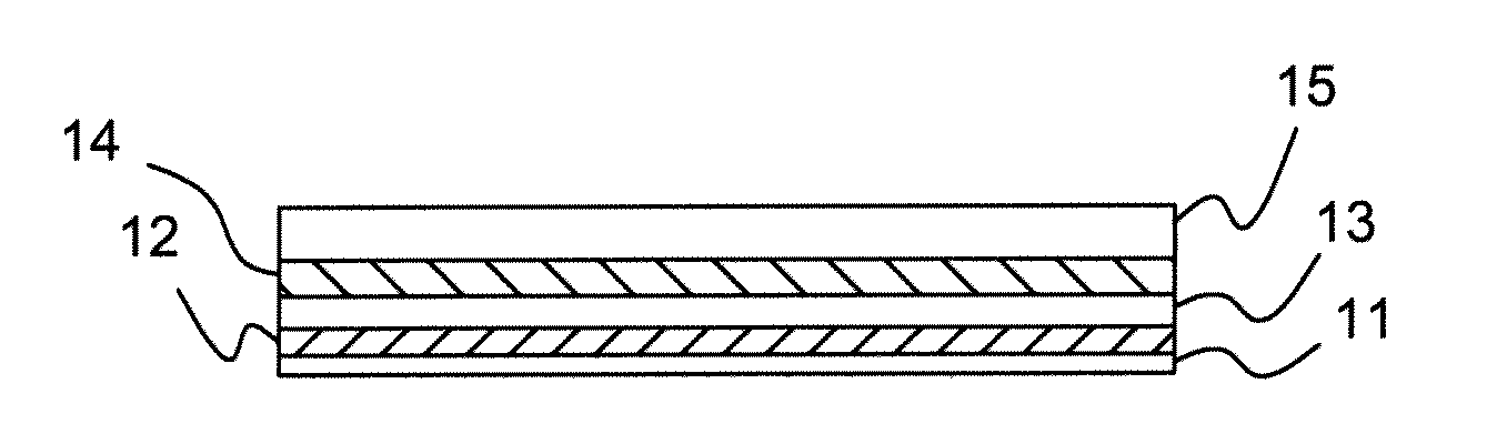
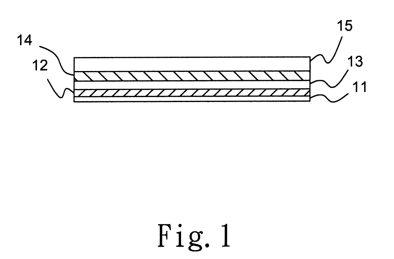
[0017]Firstly, refer to FIG. 1 for a schematic diagram of a Group III-V solar cell according to the present invention. As shown in FIG. 1, the Group III-V solar cell of the present invention comprises: a substrate 11, a first type amorphous silicon layer 12, an intrinsic amorphous silicon layer 13, a second type amorphous silicon layer 14, and a Group III-V polycrystalline semiconductor layer 15. Wherein, the substrate 11 can be made of glass, quartz, transparent plastic, sapphire, or flexible materials.

[0018]In order to receive sunlight and generate electricity, P-type semiconductor and N-type semiconductor (the first type amorphous silicon layer 12, and the second type amorphous silicon layer 14) of different conductive properties are applied on two sides of ...


PUM

PropertyMeasurementUnit
semiconductoraaaaaaaaaa
transparentaaaaaaaaaa
flexibleaaaaaaaaaa

Abstract

A Group III-V solar cell and a manufacturing method thereof, wherein, three amorphous silicon layers are formed on a substrate, which includes a first type amorphous silicon layer, an intrinsic amorphous silicon layer, and a second type amorphous silicon layer. The lattice characteristics of amorphous silicon layer are utilized, and a Group III-V polycrystalline semiconductor layer is formed on said amorphous silicon layer, such that amorphous silicon and Group III-V material are able to perform photoelectric conversion simultaneously in raising photoelectric conversion efficiency of said Group III-V solar cell effectively by means of a direct energy gap of said Group III-V material.

Description

BACKGROUND OF THE INVENTION[0001]1. Field of the Invention[0002]The present invention relates to a solar cell and a method of manufacturing the same, and in particular to a Group III-V solar cell and a method of manufacturing the same, which is capable of performing simultaneous photoelectric conversions by utilizing amorphous silicon and Group III-V materials.[0003]2. The Prior Arts[0004]With the advent of the age of high oil price and worldwide concern about global warming and environment protection, the green energy industry is thus stimulated to develop and progress rapidly. Presently, its related revenue worldwide has reached as high as several billion US dollars annually. The green energy is also referred to as a clean energy (including water resources, solar energy, wind energy, geothermal energy, and clean coal energy, etc.), and that includes almost all the environment friendly energy resources. Moreover, with the worldwide emphasis on energy conservation and carbon reducti...

Claims


Application Information

Patent Timeline
Patent Type & Authority Applications(United States)
IPC IPC(8): H01L31/0376H01L31/0352
CPCH01L31/0304H01L31/03762Y02E10/548H01L31/202Y02E10/544H01L31/076Y02P70/50
Inventor CHANG, YEE-SHYILIU, CHI-JEN
Owner CHING NEW ENERGY MACHINERY & EQUIP
Why Eureka
Try Eureka