
Non-linear, gain-based modeling of circuit delay for an electronic design automation system

a gain-based, non-linear technology, applied in the direction of cad circuit design, program control, instruments, etc., can solve the problems of complex modern electronic circuits, large design volume, and disadvantage of cell delay modeling processes, output load-based nldms, while providing delay values, and other problems

Inactive Publication Date: 2005-06-28
SYNOPSYS INC
View PDF4 Cites 20 Cited by
  • Summary
  • Abstract
  • Description
  • Claims
  • Application Information

AI Technical Summary

Benefits of technology

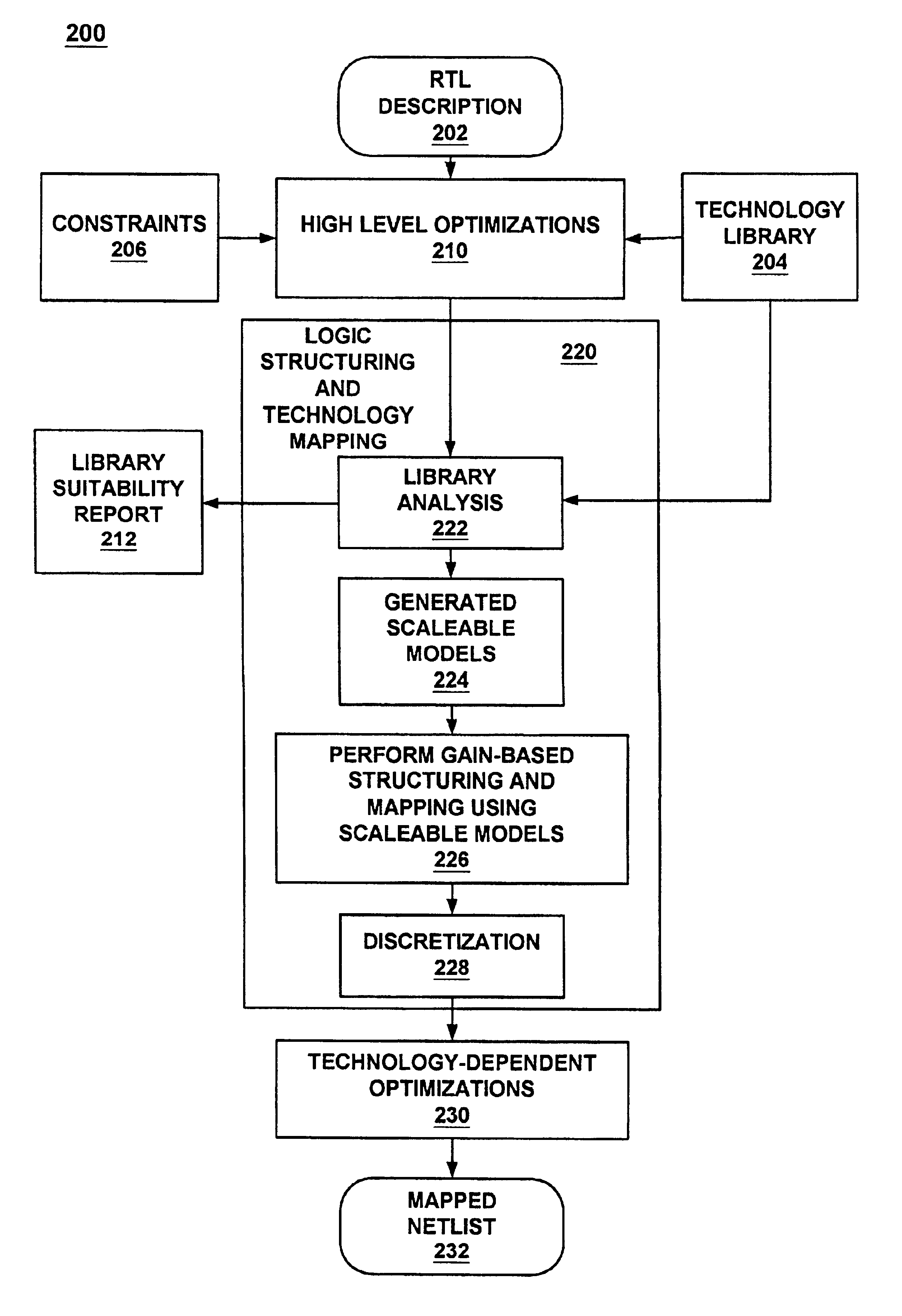
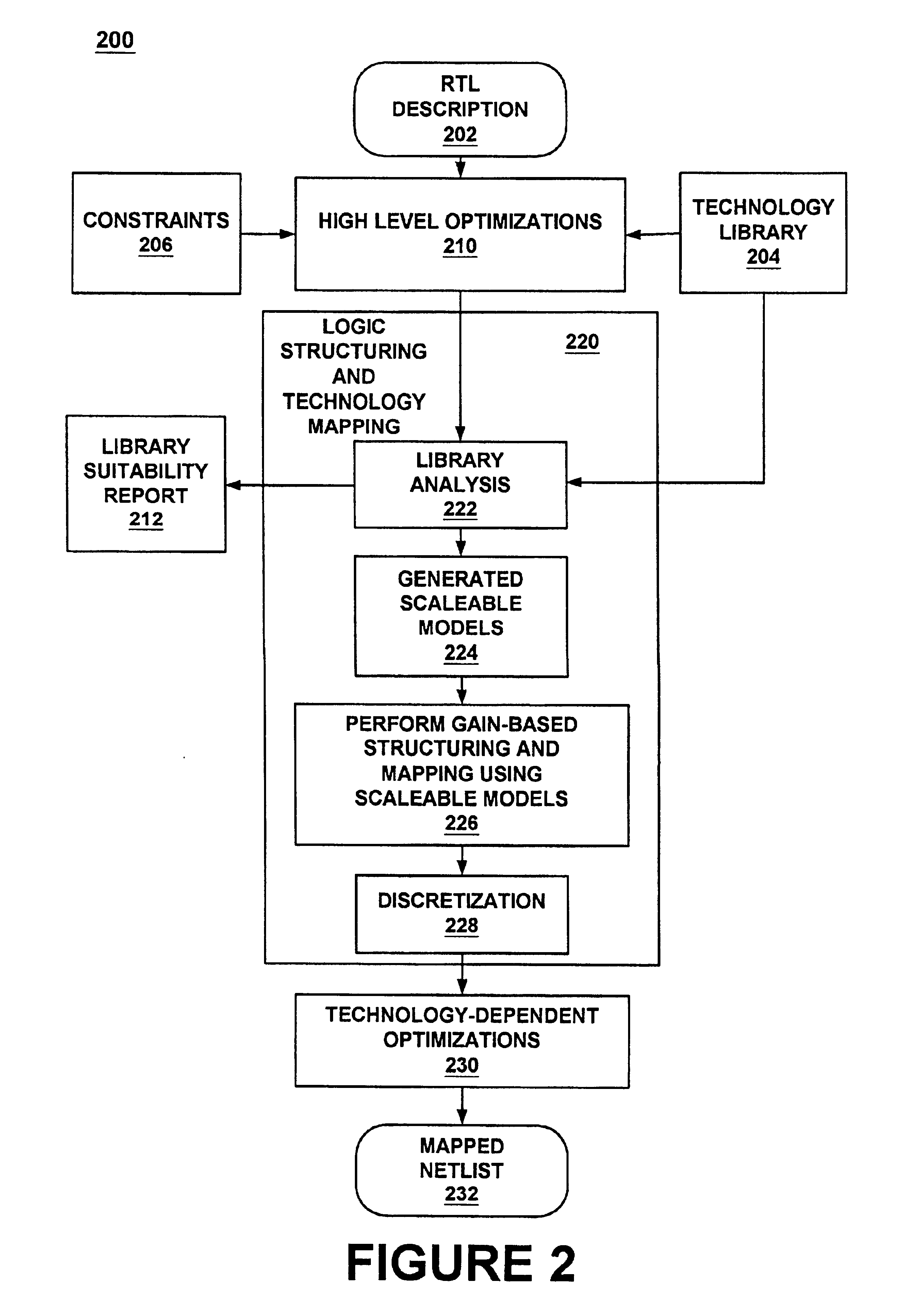
[0021]A non-linear, gain-based modeling of circuit delay within an electronic design automation (EDA) system is described herein. The present invention provides a scalable cell model for use in logic structuring and mapping for the design of integrated circuits. The scalable cell model provides a four dimensional non-linear delay model that accepts (1) input slew and (2) gain and provides (3) delay and (4) output slew information for a scalable cell. By eliminating output loading as a requirement for delay computations, the scalable model of the present invention can effectively be used to provide accurate delay (timing) information for those logic synthesis processes that precede technology dependent optimizations where the actual load of a cell is unknown. This scalable cell model considers: the impact of transition times on delay; complex gates having different input capacitances for different input pins; the impact of limited discrete cell sizes in the technology library; and design rules, e.g., maximum capacitance and maximum transition associated with gates.

Problems solved by technology

The rapid growth of the complexity of modern electronic circuits has forced electronic circuit designers to rely upon computer programs to assist and automate most steps of the circuit design process.
Typical circuits today contain hundreds of thousands or millions of individual pieces or “cells.” Such a design is much too large for a circuit designer or even an engineering team of designers to manage effectively manually.
These output load-based NLDMs, while providing delay values, have a disadvantage in the cell delay modeling processes that are performed early in the circuit synthesis process.
For instance, during early circuit synthesis processes, the output load of the cell is not known because the cells have not yet been mapped to the target technology library and, as such, the cells are not yet connected together.
Unfortunately, the output load estimates introduce inaccuracies in the overall circuit synthesis process.
The output load-based NLDMs also introduce a “Catch-22” problem in that delay modeling helps to accurately map the cells, but mapping yields the true output capacitance that is then used to accurately determine the cell's delay, etc.
However, while this simplistic delay model does have its advantages, the constant delay model does not consider several important factors when modeling the delay of a gate.
For instance, the constant delay model does not consider the impact of transition times on delay, nor does it deal effectively with complex gates with different input capacitances for different input pins.
The model also fails to take into consideration the impact of limited discrete sizes in the technology library nor of certain design rules like maximum capacitance and maximum transition associated with gates.
By not taking into consideration the above factors, the constant delay model is not as accurate as non-linear delay models.

Method used


Image

  • Non-linear, gain-based modeling of circuit delay for an electronic design automation system
  • Non-linear, gain-based modeling of circuit delay for an electronic design automation system
  • Non-linear, gain-based modeling of circuit delay for an electronic design automation system

Examples


Embodiment Construction

[0048]In the following detailed description of the present invention, a non-linear, gain-based modeling of delay using a scalable cell model, numerous specific details are set forth in order to provide a thorough understanding of the present invention. However, it will be recognized by one skilled in the art that the present invention may be practiced without these specific details or with equivalents thereof. In other instances, well known methods, procedures, components, and circuits have not been described in detail as not to unnecessarily obscure aspects of the present invention.

Cases Incorporated by Reference

[0049]The following United States co-pending patent applications are incorporated herein by reference: 1) application entitled, “Evaluation of a Technology Library for Use in an Electronic Design Automation System that Converts the Technology Library into Non-Linear, Gain-Based Models for Estimating Circuit Delay,” by M. Iyer and A. Kapoor, Ser. No. 09 / 451,467, filed Nov. 3...


PUM


Abstract

A non-linear, gain-based modeling of circuit delay within an electronic design automation system. The present invention provides a scalable cell model for use in early logic structuring and mapping for the design of integrated circuits. The scalable cell model includes a four dimensional delay model accepting input slew and gain and providing delay and output slew. By eliminating output loading as a requirement for delay computations, the scalable model of the present invention can effectively be used to provide accurate delay information for early logic synthesis processes, e.g., that precede technology dependent optimizations where the actual load of a cell is unknown. This scalable cell model considers: the impact of transition times on delay; complex gates having different input capacitances for different input pins; the impact of limited discrete cell sizes in the technology library; and design rules, e.g., maximum capacitance and maximum transition associated with gates. A technology library is analyzed and clustering is performed to select a cluster of cells for each cell group of a common functionality. A nominal input slew value is computed for all cells and a scaling factor is computed for each cell of each cluster. From each cluster, a four dimensional gain-based non-linear scalable cell model (look-up table) is generated. A default gain is computed for each scalable cell model and an area model and an input pin capacitance model are generated for each scalable cell model.

Description

[0001]This is a continuation of application Ser. No. 09 / 452,056 filed on Nov. 30, 1929, now U.S. Pat. No. 6,543,036, which is hereby incorporated by reference.BACKGROUND OF THE INVENTION[0002]1. Field of the Invention[0003]The present invention relates to the field of electronic design automation systems for designing and characterizing integrated circuits. More specifically, the present invention relates to an effective modeling method and data structure for modeling signal propagation delay of a timing arc of an integrated circuit cell.[0004]2. Related Art[0005]The rapid growth of the complexity of modern electronic circuits has forced electronic circuit designers to rely upon computer programs to assist and automate most steps of the circuit design process. Typical circuits today contain hundreds of thousands or millions of individual pieces or “cells.” Such a design is much too large for a circuit designer or even an engineering team of designers to manage effectively manually. ...

Claims


Application Information

Patent Timeline
Patent Type & Authority Patents(United States)
IPC IPC(8): G06F17/50
CPCG06F17/5022G06F30/33
Inventor IYER, MAHESHKAPOOR, ASHISH
Owner SYNOPSYS INC
Learn More