Light emitting diode

a light-emitting diode and light-emitting diode technology, applied in the direction of basic electric elements, electrical equipment, semiconductor devices, etc., can solve the problems of affecting the transmission of light from the light-emitting diode element b>4/b>, chromaticity variation, and uniform distribution, and achieve excellent productivity

Inactive Publication Date: 2005-07-05
CITIZEN ELECTRONICS CO LTD
View PDF44 Cites 195 Cited by
  • Summary
  • Abstract
  • Description
  • Claims
  • Application Information

AI Technical Summary

Benefits of technology

[0037]According to this invention, it is a structure best suitable for chi...

Problems solved by technology

It also had the problem that the fluorescent material 8 is higher than the transparent resin 9 in specific gravity and thus is difficult to disperse uniformly, causing chromaticity variations not only between different light emitting diodes but also within a single light emitting diode.
On the other hand, the lat...

Method used


Image

  • Light emitting diode
  • Light emitting diode
  • Light emitting diode

Examples


third embodiment

[0070]FIGS. 7 and 8 show the present invention. In this embodiment, the resin seal member 36 for protecting the surface side of the light emitting diode element 20 is formed in a hemispherical shape, functioning as a lens portion of convex shape to enhance the upward light-gathering power. That is, light traveling straight through the resin seal member 36 is refracted upward at the interface surface so that the enhanced light-gathering power achieves an improvement in the intensity of white luminescence.

[0071]FIG. 9 shows the fourth embodiment of the present invention. In this embodiment, a cylindrical reflecting frame 40 is arranged at the topside center of glass epoxy substrate 12. A light emitting diode element 20 is placed therein, and the surface side of this light emitting diode element 20 is protected by a hemispherical resin seal member 36 as in the third embodiment described above. The reflecting frame 40 forms an upward reflecting surface of tapered shape, with an inner pe...

fifth embodiment

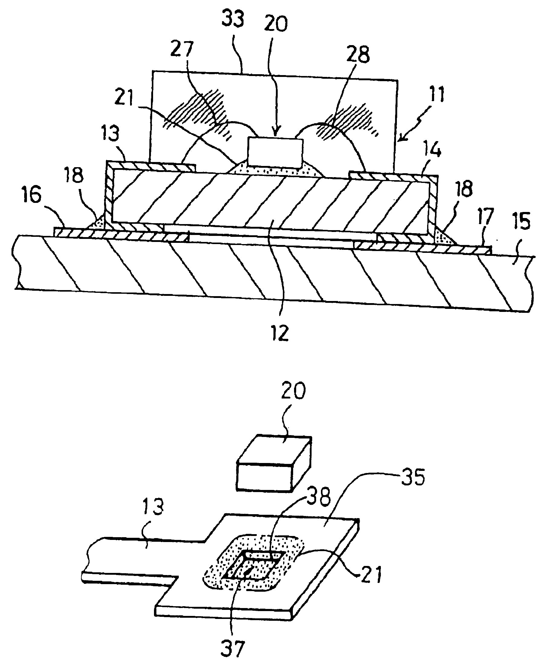
[0073]FIGS. 11 and 12 show the present invention. The light emitting diode 11 according to this embodiment uses as its base a solid-molded substrate 45 molded of a liquid crystal polymer. A bowl-shaped cup portion 46 is formed in the center of the solid-molded substrate 45. A cathode and an anode, or topside electrodes, 13 and 14 are formed on the top surface of the solid-molded substrate 45 to the right and left astride a slit 47 in the center. On the inner periphery of the above-mentioned cup portion 46 are formed a reflecting surface 48 which is integrally molded with the topside electrodes 13 and 14 mentioned above. This reflecting surface 48 is hollowed round at the bottom 49 of the cup portion 46, so that the solid-molded substrate 45 is seen directly. Then, the same fluorescent material containing layer 21 as described above is applied to this bottom 49, and the light emitting diode element 20 is placed on and fixed to the same. Incidentally, a pair of electrodes of the light...

seventh embodiment

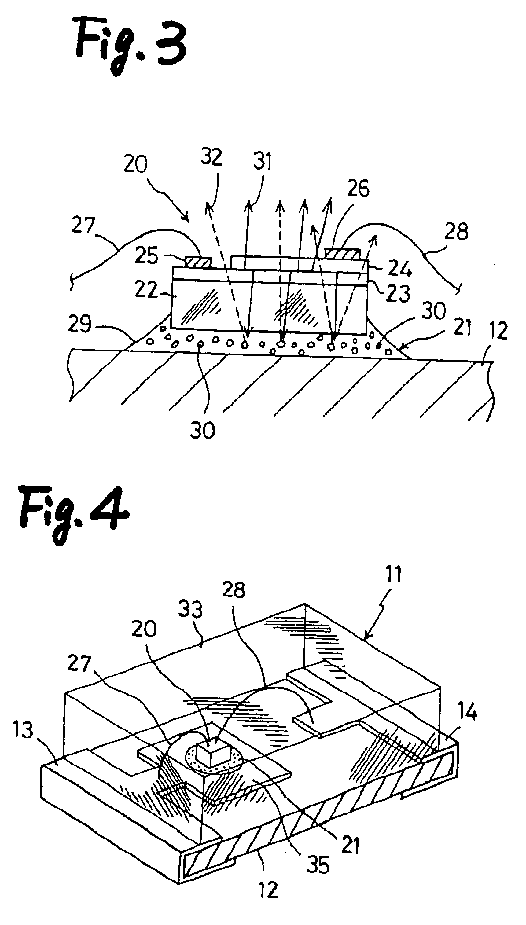
[0077]FIG. 14 shows the present invention. In this embodiment, a fluorescent material containing layer 39 is formed thinly on the top side of a rectangular-solid-shaped resin seal member 33 so as to allow color adjustment on the top surface. The fluorescent material containing layer 39 is composed of a fluorescent material 30 of the above-mentioned yttrium type or a different fluorescent material, dispersed into an organic solvent. It may be printed as paint on the top surface of the resin seal member 33, or formed into a sheet and pasted. The fluorescent material containing layer 39 is formed thinly, which makes it possible to minimize a drop in light transmittance in the resin seal member 33.


PUM


Abstract

A light emitting diode comprising a light emitting diode element 20 mounted on a glass epoxy substrate 12, this light emitting diode element 20 being protected at its surface side by a resin seal member 33, in which: a light emitting diode element for blue luminescence, formed of gallium nitride type compound semiconductor is used as the above-mentioned light emitting diode element 20; and a fluorescent material containing layer 21 composed of a fluorescent material containing layer 21 composed of a fluorescent material dispersed into an adhesive is arranged on the back side of this light emitting diode element. On the back side of the light emitting diode element 20, blue luminescence is converted in wavelength to produce white luminescence of high intensity.

Description

[0001]This is a continuation of copending parent application Ser. No. 09 / 763,421, nationalized Feb. 22, 2001, of which the international application was filed PCT / JP00 / 04006, filed Jun. 20, 2000.FIELD OF THE INVENTION[0002]The present invention relates to a light emitting diode of wavelength conversion type, and more particularly to a type of light emitting diode which converts blue luminescence into white.BACKGROUND OF THE INVENTION[0003]Conventionally, among this kind of light emitting diodes of wavelength conversion type are known the one shown in FIG. 22 (Japanese Patent No. 2900928) and the one shown in FIG. 23 (Japanese Patent Laid-Open Publication No. Hei 7-99345). The former one is a light emitting diode 1 of lead frame type, having a structure in which: a recess 3 is arranged in a metal stem 2, one of the lead frames; a light emitting diode element 4 made of gallium nitride type compound semiconductor is placed on and fixed to this recess 3; and this light emitting diode el...

Claims


Application Information

Patent Timeline
IPC IPC(8): H01L33/00H01L33/48H01L33/50
CPCH01L33/486H01L33/508H01L24/29H01L25/0753H01L2224/73265H01L2224/48091H01L2924/00014H01L2224/32225H01L2224/48227H01L2224/48247H01L2224/49107H01L2224/92247H01L2924/00012H01L2924/181H01L2924/12041H01L24/73H01L2924/00
Inventor FUKASAWA, KOICHIMIYASHITA, JUNJITSUCHIYA, KOUSUKE
Owner CITIZEN ELECTRONICS CO LTD
Why Eureka
Try Eureka