Image sensor

a solid-state image and sensor technology, applied in the field of image sensors, can solve the problems of fixed pattern noise, deterioration of picture quality, fpn, etc., and achieve the effect of reducing ktc noise, wide opening ratio, and small element siz

Active Publication Date: 2005-07-05
SOCIONEXT INC
View PDF10 Cites 12 Cited by
  • Summary
  • Abstract
  • Description
  • Claims
  • Application Information

AI Technical Summary

Benefits of technology

[0018]An object of the present invention is to provide an X-Y address type solid-state image pickup device which has a small element size and a wide opening ratio, and can reduce the kTC noise.
[0019]The above object can be achieved by an X-Y address type solid-state image pickup device characterized by comprising a pixel region including a photoelectric transducer for performing photoelectric conversion of incident light, a reset transistor for resetting the photoelectric transducer, an amplifying transistor for converting an electric charge stored in the photoelectric transducer into a voltage, and a horizontal selection transistor for outputting the voltage as image data to a vertical selection line on the basis of a horizontal selection signal outputted to a horizontal line, and a kTC noise reduction circuit for reducing a kTC noise generated at a time of the resetting.

Problems solved by technology

However, in the conventional APS structure in which the charge storage capacitance photodiode 400 and the source follower amplifier 404 are mounted, there is a problem that a fixed pattern noise (FPN) in which a DC level of a signal voltage is changed by fluctuation of a threshold voltage VT or the like, is generated and picture quality is deteriorated.
Thus, there remains a problem that the kTC noise generated at random from the photodiode 400 in a reset period can not be removed by the CDS circuit, and the S / N ratio is deteriorated as compared with the CCD solid-state image pickup device.
However, in the structure of the conventional CMOS image sensor shown in FIG. 7, as described above, although the FPN and the kTC noise can be reduced, there is a problem that the element structure becomes complicated.
The element structure of the pixel shown in FIG. 7 has a problem that as compared with the element structure of the pixel shown in FIG. 6, the number of the transistors is increased, the pixel portion becomes complicated, and the opening ratio (fill factor) of a light receiving portion is lowered.
However, in this structure, since it becomes necessary to arrange the wiring line 416 in the pixel region, there arises a problem that an opening ratio is not made wide.
As described above, the CMOS image sensor shown in FIG. 6 has the problem that the kTC noise can not be reduced.
On the other hand, the CMOS image sensors shown in FIGS. 7 and 8 have the problem that in exchange for reduction of the kTC noise, the element size becomes large and a wide opening ratio can not be obtained.

Method used


Image

  • Image sensor
  • Image sensor
  • Image sensor

Examples


Embodiment Construction

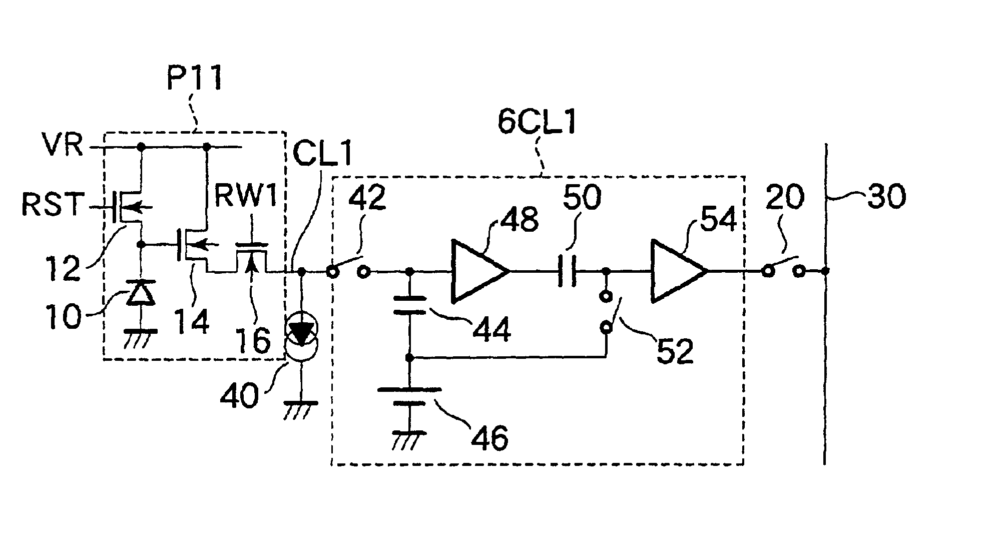
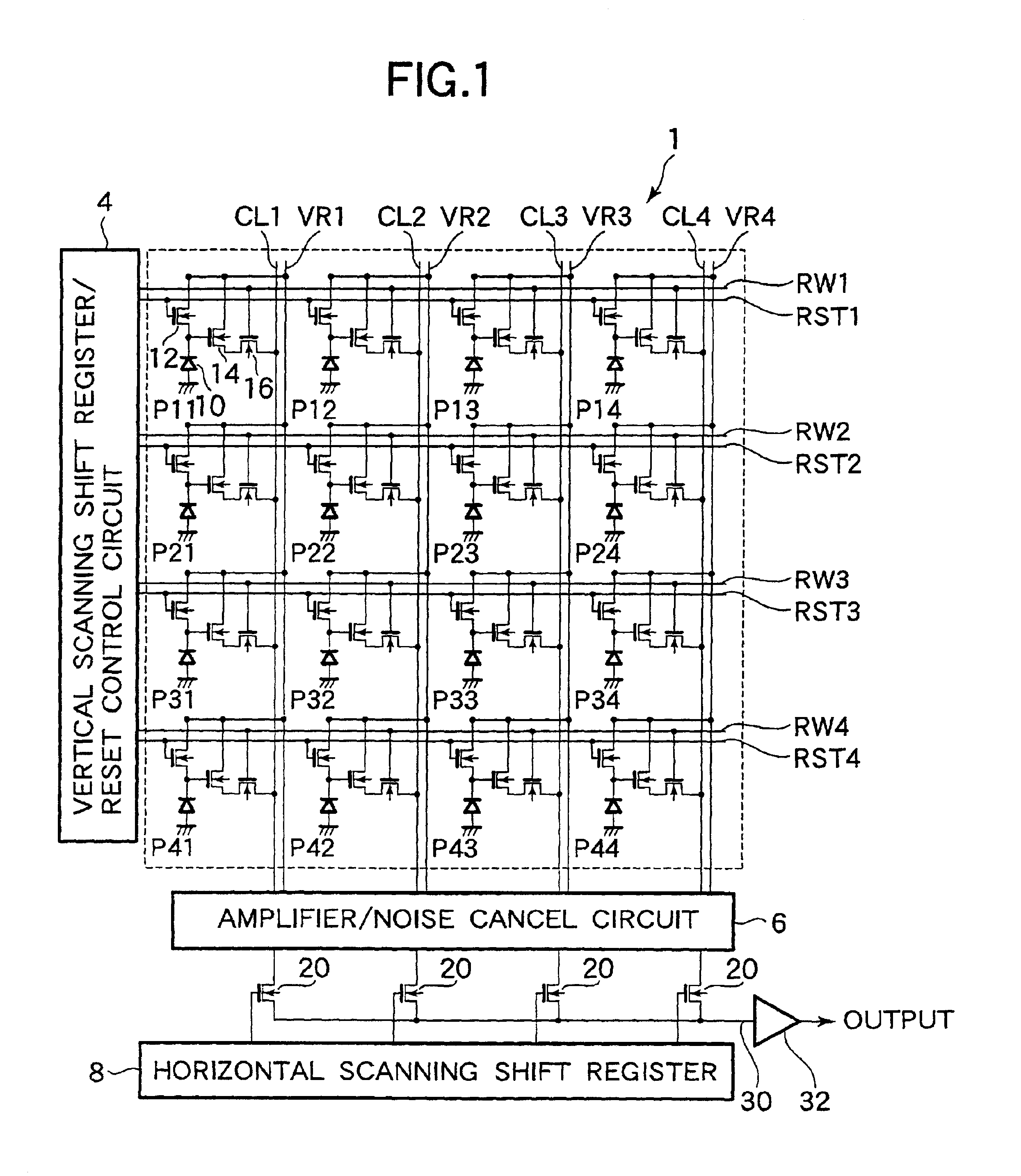
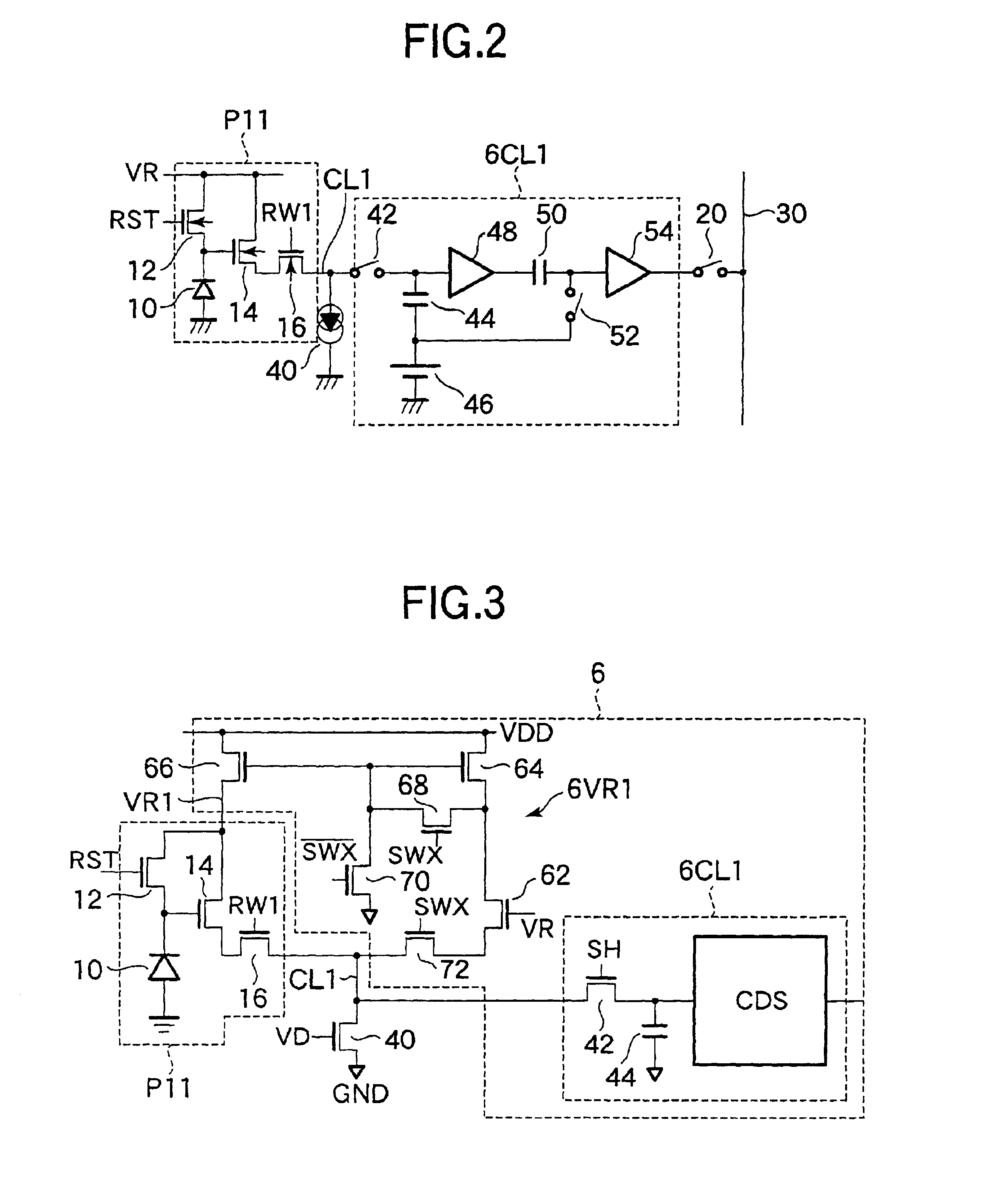
[0028]An X-Y address type solid-state image pickup device according to an embodiment of the present invention will be described with reference to FIGS. 1 to 5. First, a rough structure of a CMOS image sensor as the X-Y address type solid-state image pickup device according to the embodiment will be described with reference to FIG. 1. FIG. 1 shows a circuit example of 4×4 pixels of a CMOS image sensor 1 including a pixel array of m rows and n columns. A plurality of pixel regions P11 to P44 are arranged in a matrix form, and a plurality of vertical selection lines CL1 to CL4 and a plurality of horizontal selection lines RW1 to RW4 are arranged vertically and horizontally. A photodiode 10 as a photoelectric transducer is formed in each of the pixel regions P11 to P44. As the photoelectric transducer, for example, a photo gate may be used instead of the photodiode 10.

[0029]The CMOS image sensor 1 has an APS structure in which a source follower amplifier 14 constituted by, for example, ...


PUM


Abstract

The invention relates to an X-Y address type solid-state image pickup device manufactured by a CMOS process, and has an object to provide an X-Y address type solid-state image pickup device which has a small element size and a wide opening ratio, and can reduce a kTC noise. A photodiode 10, a reset transistor 12, a source follower amplifier 14, and a horizontal selection transistor 16 are formed in each of pixel regions Pmn. A kTC noise reduction circuit 6VR1 for reducing a kTC noise and a CDS circuit 6CL1 are formed outside of the pixel regions Pmn. A differential amplifier is constituted by a first differential transistor 62 of the kTC noise reduction circuit 6VR1 and the source follower amplifier 14 in each of the pixel regions Pmn.

Description

BACKGROUND OF THE INVENTION[0001]1. Field of the Invention[0002]The present invention relates to a solid-state image pickup device constituted by semiconductor elements, and particularly to an X-Y address type solid-state image pickup device manufactured by a CMOS process.[0003]2. Description of the Related Art[0004]In recent years, solid-state image pickup devices are incorporated in various products, such as digital still cameras, digital video cameras, or portable telephones, and are used in large quantities. The solid-state image pickup device is roughly classified into a CCD (Charge Coupled Device) solid-state image pickup device constituted by a charge transfer image sensor, and an X-Y address type solid-state image pickup device in which an image sensor is constituted by, for example, CMOS (Complementary Metal Oxide Semiconductor) transistors. The X-Y address type solid-state image pickup device using a CMOS image sensor (hereinafter suitably abbreviated to a CMOS image senso...

Claims


Application Information

Patent Timeline
Patent Type & Authority Patents(United States)
IPC IPC(8): H04N3/15H04N5/217H01L31/10H01L27/146H04N5/335H04N5/365H04N5/369H04N5/374H04N5/378
CPCH04N5/363H04N25/65H04N25/76
Inventor UDO, SHINYAKOKUBUN, MASATOSHITSUCHIYA, CHIKARAYAMAMOTO, KATSUYOSI
Owner SOCIONEXT INC
Why Eureka
Try Eureka