Multilayer capacitor

Active Publication Date: 2005-07-05
TDK CORPARATION
View PDF13 Cites 40 Cited by
  • Summary
  • Abstract
  • Description
  • Claims
  • Application Information

AI Technical Summary

Benefits of technology

[0015]The present invention has as its object the provision of a multilayer capacitor capable of greatl

Problems solved by technology

In recent years, CPUs (central processing units) used for data processing apparatuses have become higher in operating frequency and remarkably increased in current consumption due to the improvement in processing speeds and higher integration.
It has become extremely difficult to keep voltage fluctuations accompanying current fluctuations to within tolerances of the power sources.
Along with the increasingly higher operating frequencies of today's CPUs,

Method used


Image

  • Multilayer capacitor
  • Multilayer capacitor
  • Multilayer capacitor

Examples


first embodiment

[0149

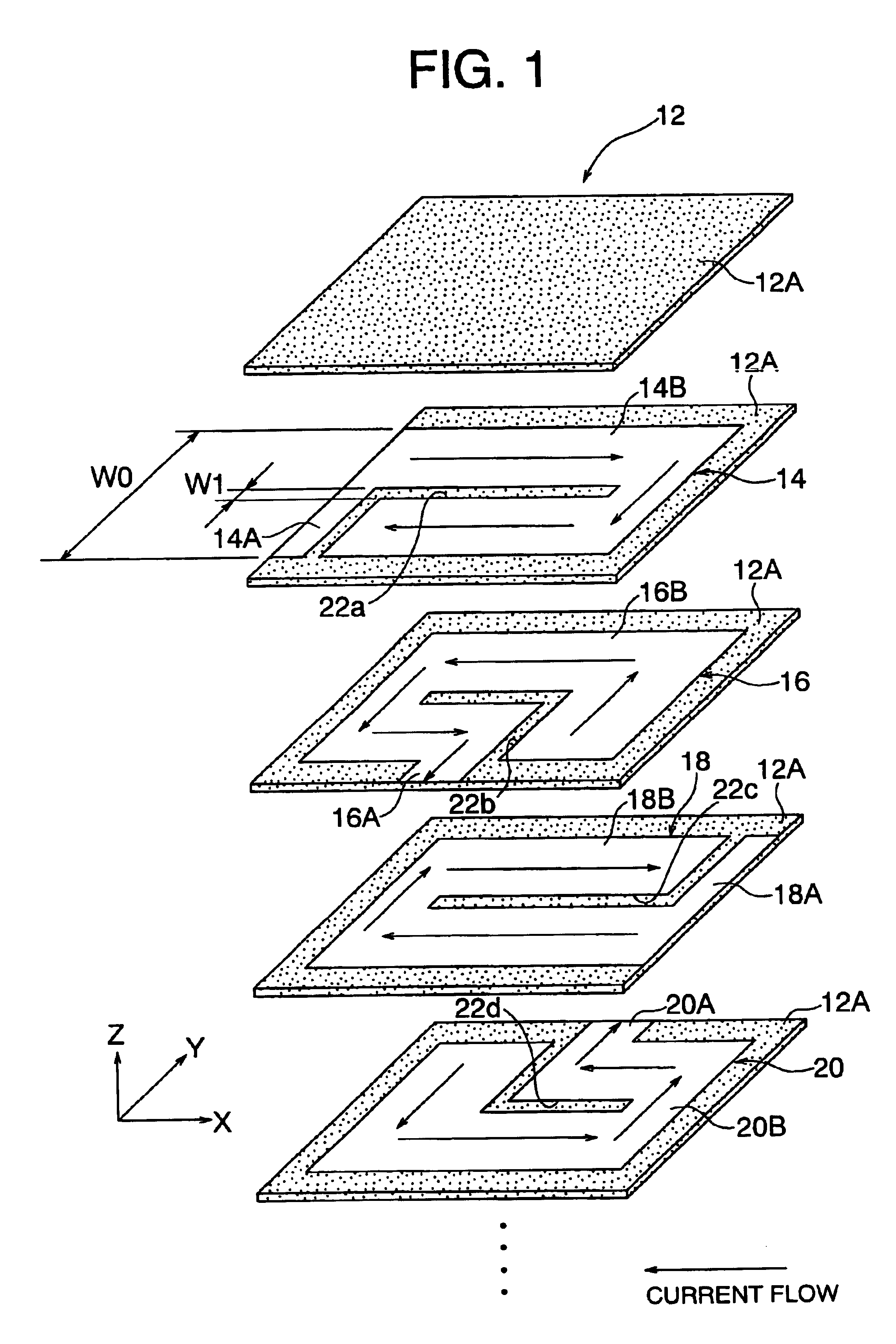
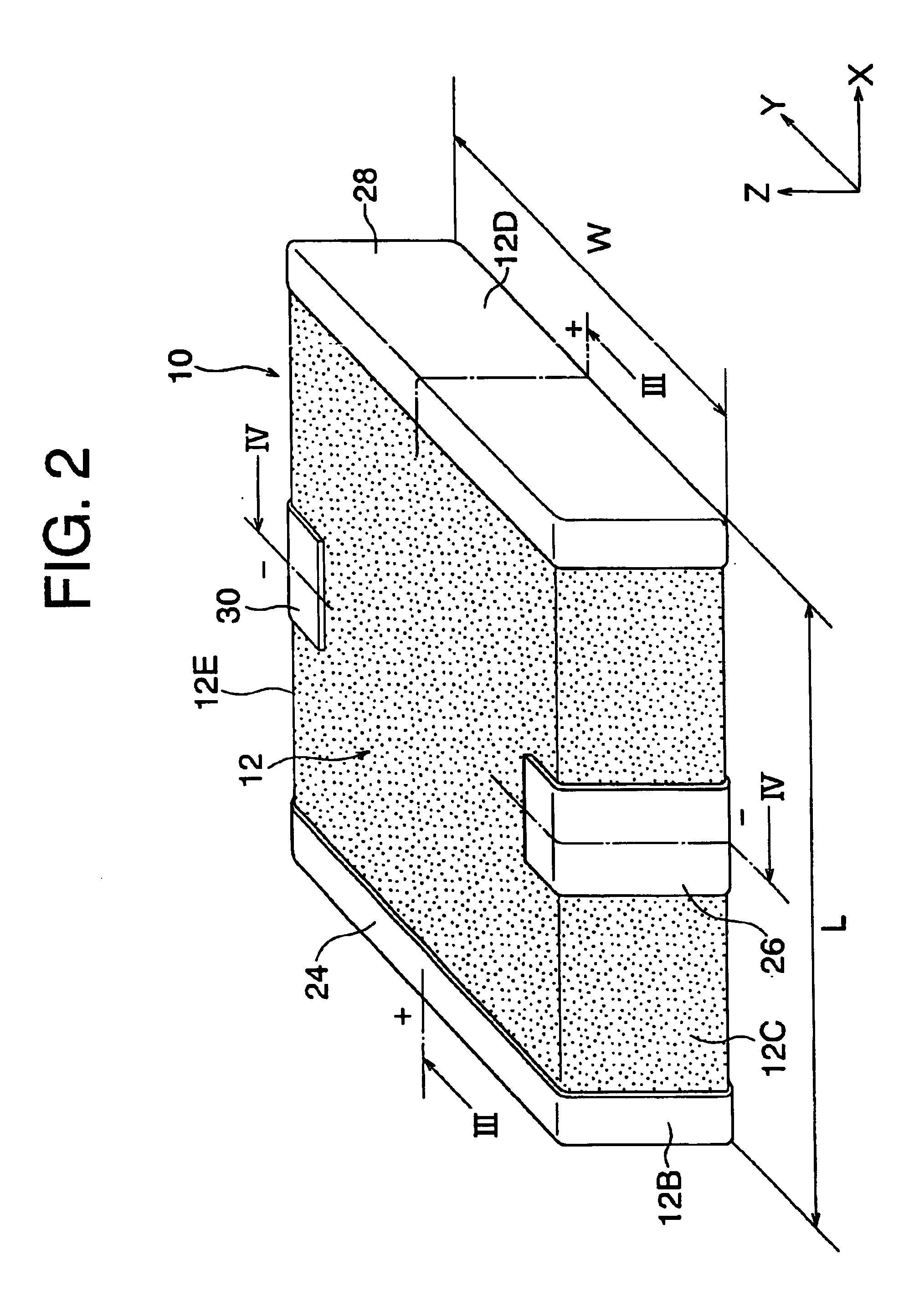
[0150]A multilayer ceramic capacitor as an embodiment of the multilayer capacitor according to the present invention (hereinafter simply referred to as a “multilayer capacitor”) 10 is shown in FIG. 1 to FIG. 5. As shown in these figures, the multilayer capacitor 10 is comprised of, as a main part, a dielectric body 12 comprised of a rectangular parallelepiped shaped sintered body obtained by sintering a stack of a plurality of ceramic green sheets as dielectric sheets (which become ceramic layers 12A after firing).

[0151]As shown in FIG. 1, FIG. 3 and FIG. 4, a planar shaped first internal conductor layer 14, wherein the plane is along the X-axis and Y-axis, is arranged at a position of a predetermined height in the stacking direction Z of the ceramic layers (dielectric layers) 12A in the dielectric body 12. In the dielectric body 12, the same planar shaped second internal conductor layer 16 is arranged below the internal conductor layer 14 over the ceramic layer 12A.

[0152]In th...

second embodiment

[0179

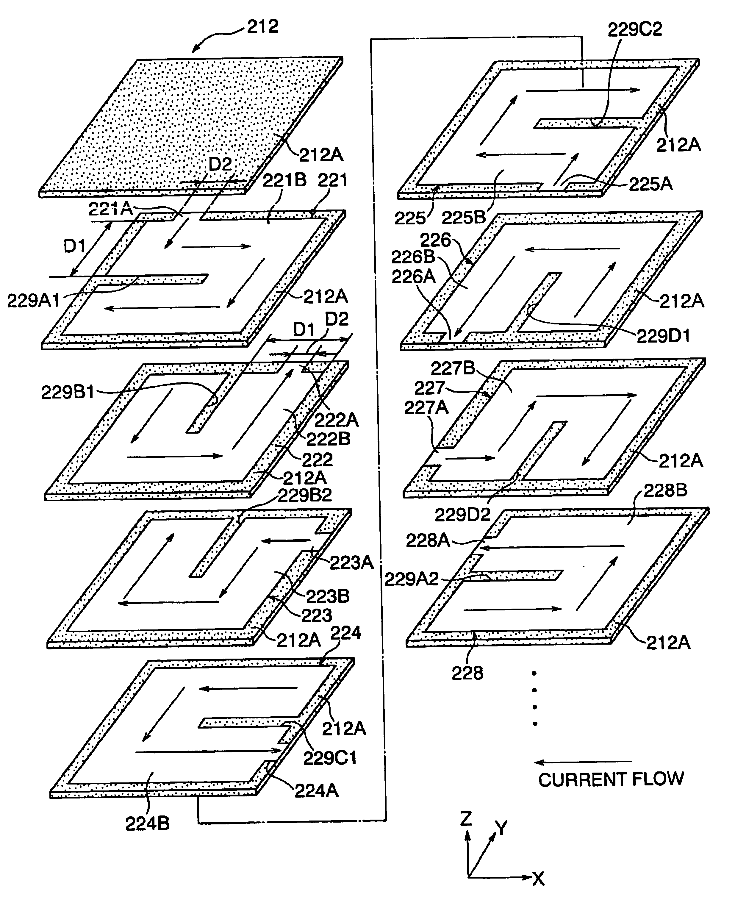
[0180]Below, a multilayer capacitor accordance to a second embodiment of the present invention will be explained based on the drawings. The multilayer ceramic capacitor (hereinafter, simply referred to as a multilayer capacitor) 210 according to the present embodiment is shown in FIG. 11 to FIG. 14. As shown in these figures, the multilayer capacitor 210 is comprised of, as a main part, a dielectric body 212 comprised of a rectangular parallelepiped shaped sintered body obtained by sintering a stack of a plurality of ceramic green sheets as dielectric sheets (which become ceramic layers 212A after firing).

[0181]As shown in FIG. 11 and FIG. 13, a planar shaped first internal conductor layer 221, wherein the plane is along the X-axis and Y-axis, is arranged at a position of a predetermined height of the dielectric body 212. In the dielectric body 212, the same planar shaped second internal conductor layer 222 is arranged below the first internal conductor layer 221 in the stackin...

third embodiment

[0216

[0217]A multilayer ceramic capacitor (hereinafter, simply referred to as a multilayer capacitor) 310 as a third embodiment of the multilayer capacitor according to the present invention is shown in FIG. 16 to FIG. 21. As shown in the figures, the multilayer capacitor 310 is comprised of, as a main part, a dielectric body 312 comprised of a rectangular parallelepiped shaped sintered body obtained by sintering a stack of a plurality of ceramic green sheets as dielectric sheets (which become ceramic layers 312A after firing).

[0218]As shown in FIG. 16 and FIG. 18, a planar shaped first internal conductor layer 321, wherein the plane is along the X-axis and Y-axis, is arranged at a position of a predetermined height in the stacking direction Z of the ceramic layers (dielectric layers) 312A in the dielectric body 312. On the ceramic layer 312A to be formed a first conductor layer 321, a fifth internal conductor layer 325 is formed adjacent to the first internal conductor layer 321 by...


PUM

PropertyMeasurementUnit
Widthaaaaaaaaaa

Abstract

Internal dielectric layers isolated between them by a ceramic layer are arranged in a dielectric body, other internal conductor layers also isolated between them by a ceramic layer are arranged in the dielectric body by being isolated from the above internal conductor layers. Each of the all internal conductor layers is formed with a cut part, and a channel part is formed around the cut part, and the channel parts are arranged so that currents flow in mutually reverse directions between channel parts of internal conductor layers adjoining across a ceramic layer. Consequently, the equivalent serial inductance of the multilayer capacitor is largely reduced and fluctuations of a power source voltage of a CPU is made small.

Description

BACKGROUND OF THE INVENTION[0001]1. Field of the Invention[0002]The present invention relates to a multilayer capacitor wherein the equivalent serial inductance (ESL) is greatly reduced, more particularly relates to a multilayer ceramic capacitor capable of reducing the voltage fluctuations of a CPU power source.[0003]2. Description of the Related Art[0004]In recent years, CPUs (central processing units) used for data processing apparatuses have become higher in operating frequency and remarkably increased in current consumption due to the improvement in processing speeds and higher integration. Along with this, there is a trend toward reduction of the power consumption so as to reduce the operating voltage. Therefore, in power sources for supplying power to CPUs, faster and larger current fluctuations occur. It has become extremely difficult to keep voltage fluctuations accompanying current fluctuations to within tolerances of the power sources.[0005]Therefore, as shown in FIG. 7, ...

Claims


Application Information

Patent Timeline
IPC IPC(8): H01G4/30H01G4/005H01G4/228H01G4/12H01G4/06H01G4/012H01G4/232H01G4/40
CPCH01G4/012H01G4/40H01G4/30H01G4/232
Inventor TOGASHI, MASAAKIIMAI, ICHIROU
Owner TDK CORPARATION
Why Eureka
Try Eureka