Method for driving a liquid crystal display device

a liquid crystal display and display device technology, applied in the direction of static indicating devices, identification means, instruments, etc., can solve the problems of lowering the aperture ratio due to the orientation disturbance of liquid crystal molecules, the difficulty of applying the correct voltage on the liquid crystal, and the flicker becomes larger, etc., to achieve the effect of reducing the brightness of the screen, reducing the aperture ratio, and small strength

Active Publication Date: 2009-04-28
HANNSTAR DISPLAY CORPORATION
View PDF4 Cites 7 Cited by
  • Summary
  • Abstract
  • Description
  • Claims
  • Application Information

AI Technical Summary

Benefits of technology

[0024]Accordingly, it is an object of the present invention to provide a liquid crystal display device which provides a high aperture ratio.
[0025]Another object of the present invention is to provide a liquid crystal display device which is capable reducing the unevenness of brightness over the screen and flicker.
[0044]The liquid crystal display device according to the present invention achieves a high aperture ratio of pixels and reduction in brightness unevenness on screen and flickering and is preferably used for liquid crystal projectors.
[0048]Since the polarities of the video signals supplied to adjacent pixels relative to common electrode are the same in accordance with the present invention, lateral electric field which occurs in the pixel boundaries is small in strength, so that the region at which the orientation of the liquid crystal molecules is disturbed can be reduced. Therefore, portions which could not be utilized in the prior art can be used as an aperture, thereby achieving a high aperture ratio.
[0049]In accordance with the present invention, video signals having the same polarity relative to the common electrode are supplied to every divided pixel regions while the polarities of the video signals supplied to adjacent pixel regions are different. The order of writing video signals into the pixel matrix is determined so that the pixel regions are selected to make the polarity of the video signal to be written different every one horizontal period. Accordingly, the polarity of the video signals supplied to the data lines is alternately changed every one horizontal period. Thus, the average value of the drain-to-source voltage applied to pixel transistors in all positions in the pixel matrix can be uniformed. As a result, the brightness non-uniformity on the screen and flickering can be reduced.
[0050]In accordance with the present invention, the period which is taken to write signals of one screen to the liquid crystal display device can be shortened, so that voltage fluctuations due to photo-leakage current of pixel transistors can be reduced. As a result, flickering can be reduced.

Problems solved by technology

The reason resides in that continuous application of a voltage having a DC (direct current) component to a liquid crystal causes impurity-ions contained in the liquid crystal material at a very small amount are gathered around an electrode, thereby making it difficult to apply a correct voltage upon the liquid crystal.
The lowering of the aperture ratio due to orientation disturbance of liquid crystal molecules becomes serious particularly in such a high-resolution liquid crystal display device having a pixel pitch of 20 μm or less.
However, this frame inversion driving method has a problem that the flicker becomes larger.
This method utilizes a fact that flickering is hard to perceive for human eyes when the screen is rewritten at a high speed.

Method used


Image

  • Method for driving a liquid crystal display device
  • Method for driving a liquid crystal display device
  • Method for driving a liquid crystal display device

Examples


second embodiment

[0108]Another embodiment of the present invention will now be described. An configuration wherein the pixel matrix is divided into 4 is shown in FIG. 8 as an example wherein the pixel matrix is divided into a number larger than 2. In the present invention, the pixel matrix 10 comprises pixel regions 10-1 through 10-4. FIG. 9 is a timing chart showing the operation of the configuration in FIG. 8. In FIG. 9, Dj denotes the signal voltage of the data lines 12, G1 through Gk, Gk+1 through G2k, G2k+1 through G3k, G3k+1 through G4k denote voltage wave forms of the gate lines of the first, second, third and fourth pixel regions, respectively. P1, j through Pk, j, Pk+1, j through P2k, j, P2k+1, j through P3k, j, P3K+1, j through P4k, j denote the potentials of the pixel electrodes in first to k-th pixel row (first pixel region), k+1 to 2K-th pixel rows (second pixel region), 2K+1 to 3k-th pixel rows (third pixel region9, and 3k+1 to 4k-th pixel rows (fourth pixel region), respectively. Hori...

third embodiment

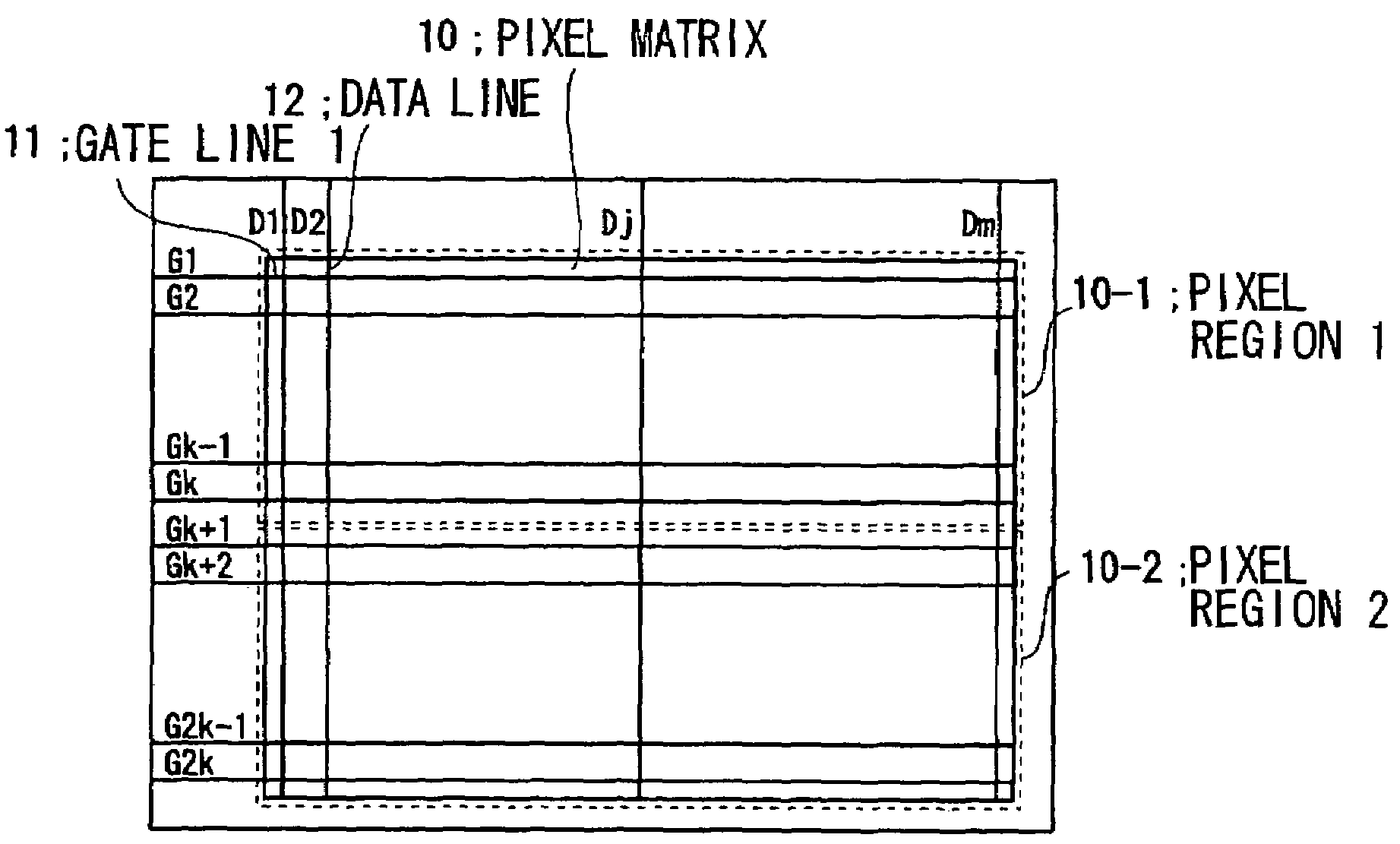
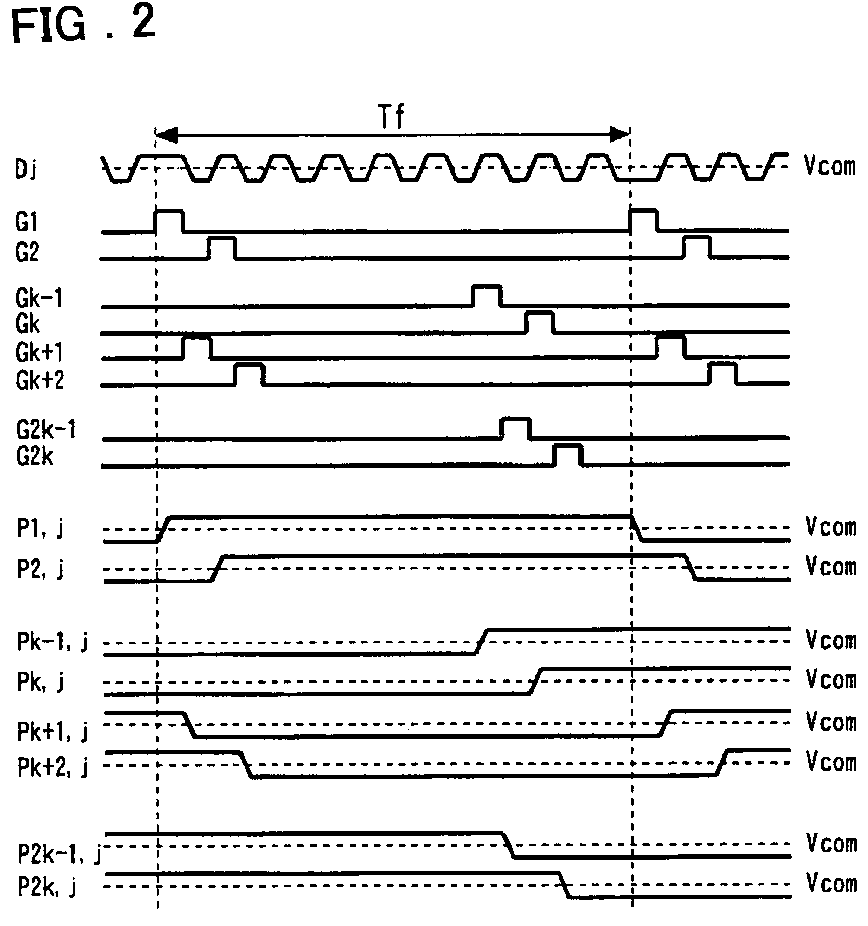
[0116]A drive circuit for practicing the above-mentioned driving method will be described. FIG. 10 shows the configuration of the liquid crystal display device of the present invention. The liquid crystal display device comprises a pixel matrix 10 including pixels each comprising a pixel transistor 13, pixel capacitor 15, and storage capacitor 14 as shown in FIG. 3. Each pixel is disposed in each of intersections of the data lines denoted as D1 through Dm with the gate lines denoted as G1 through G2k. A liquid crystal is sandwiched between a matrix substrate on which the pixel matrix is formed and an opposite substrate (not shown) on which a common electrode common to the pixel electrodes of pixels is provided. The pixel matrix is divided into plurality of pixel regions which are in parallel with the gate lines. In an example shown in FIG. 10, the pixel matrix is divided into two pixel regions 10-1 and 10-2. It is of course that the pixel matrix may be divided to a desired number of...

fourth embodiment

[0127]In the embodiment shown in FIG. 10, the gate driver circuit 30 is disposed on only one side of the pixel matrix. The present invention is limited to such a configuration. In a fourth embodiment, the gate driver circuits 30-1 and 30-2 may be disposed on the both sides of the pixel matrix as shown in FIG. 17.

[0128]A fifth embodiment of the present invention will now be described. In the fifth embodiment, a pre-charge circuit 40 which is capable of performing preliminarily charging / discharge of the data line 11 (all data lines) of the pixel matrix to a desired voltage every one horizontal period is provided as shown in FIG. 18.


PUM

PropertyMeasurementUnit
frequencyaaaaaaaaaa
polaritiesaaaaaaaaaa
voltageaaaaaaaaaa

Abstract

In a liquid crystal display device, a pixel matrix is divided into a plurality of pixel regions in unit of pixel column. The pixel matrix is driven so that video signals having the same polarity are written into every divided pixel regions and video signals having different polarities are written into adjacent pixel regions during a vertical period during which signals of one screen are written and the polarity of the video signals is alternately changed every vertical period.

Description

FIELD OF THE INVENTION[0001]The present invention relates to a liquid crystal display device and in particular to an active matrix type liquid crystal display device and an electronic device having the same.BACKGROUND OF THE INVENTION[0002]In liquid crystal display devices, it is necessary to conduct an alternating current drive in which the polarity of a voltage applied to a liquid crystal is alternately changed for every frame. The reason resides in that continuous application of a voltage having a DC (direct current) component to a liquid crystal causes impurity-ions contained in the liquid crystal material at a very small amount are gathered around an electrode, thereby making it difficult to apply a correct voltage upon the liquid crystal. Therefore, conventional active matrix type liquid crystal display devices use the driving method as follows:[0003]A gate line inversion driving method for alternately changing the polarity of a signal which is written to pixels with respect t...

Claims


Application Information

Patent Timeline
Patent Type & Authority Patents(United States)
IPC IPC(8): G09G3/36G02F1/133G09F9/30G09G3/20
CPCG09G3/3614G09G3/3648G09G2310/02G09G2320/0233
Inventor SEKINE, HIROYUKI
Owner HANNSTAR DISPLAY CORPORATION
Why Eureka
Try Eureka