High efficiency triple well charge pump circuit

a charge pump and triple well technology, applied in the field of integrated circuits, can solve the problems of reducing efficiency, reducing the threshold voltage of the charge transfer mos device, and limited maximum output voltage of the conventional charge pump circuit, and achieves low power supply operation, small layout area, and high boosted voltage and current output.

Inactive Publication Date: 2005-07-05
HALO LSI INC
View PDF16 Cites 78 Cited by
  • Summary
  • Abstract
  • Description
  • Claims
  • Application Information

AI Technical Summary

Benefits of technology

[0020]It is still further an objective of the present invention to reduce the body effect to the charge transfer MOSFET device by the transfer of the boosted source voltage by an auxiliary MOSFET device to the P-well and N-well of each stage, which is then floated when the auxiliary device is turned off.
[0024]The auxiliary device, which is used for pre-charging a voltage on the gate of the charge transfer device, couples the input signal of each stage to the gate of the charge transfer device; and therefore, increases the boost coupling effect on the charge transfer MOS device, which results in increasing a signal level at the source (output) of the charge transfer device. The auxiliary device, that is used for buffering the drain of the charge transfer device from the P-well and the N-well, couples the drain voltage of the charge transfer device to the P-well and the deep N-well to reduce the body effect and to improve capacitive coupling effect on the drain of charge transfer MOSFET device by reducing the effects of the P-well and Deep N-well parasitic capacitance.

Problems solved by technology

The technique of prior art has been widely used, but suffers from degradation in threshold voltage of charge transfer MOS devices during its operation.
As a result the maximum output voltage of the conventional charge pump circuit is limited and the efficiency decreases as the number of stages increase, especially for low power supply voltage.
The parasitic capacitance of the P-well and the deep N-well negatively affects the boosting voltage coupled to the drain of the charge transfer MOS device when the boosting clock signal is on.
These two effects cause a degradation of efficiency of the charge pump circuit, especially at low power supply voltages.

Method used


Image

  • High efficiency triple well charge pump circuit
  • High efficiency triple well charge pump circuit
  • High efficiency triple well charge pump circuit

Examples


Embodiment Construction

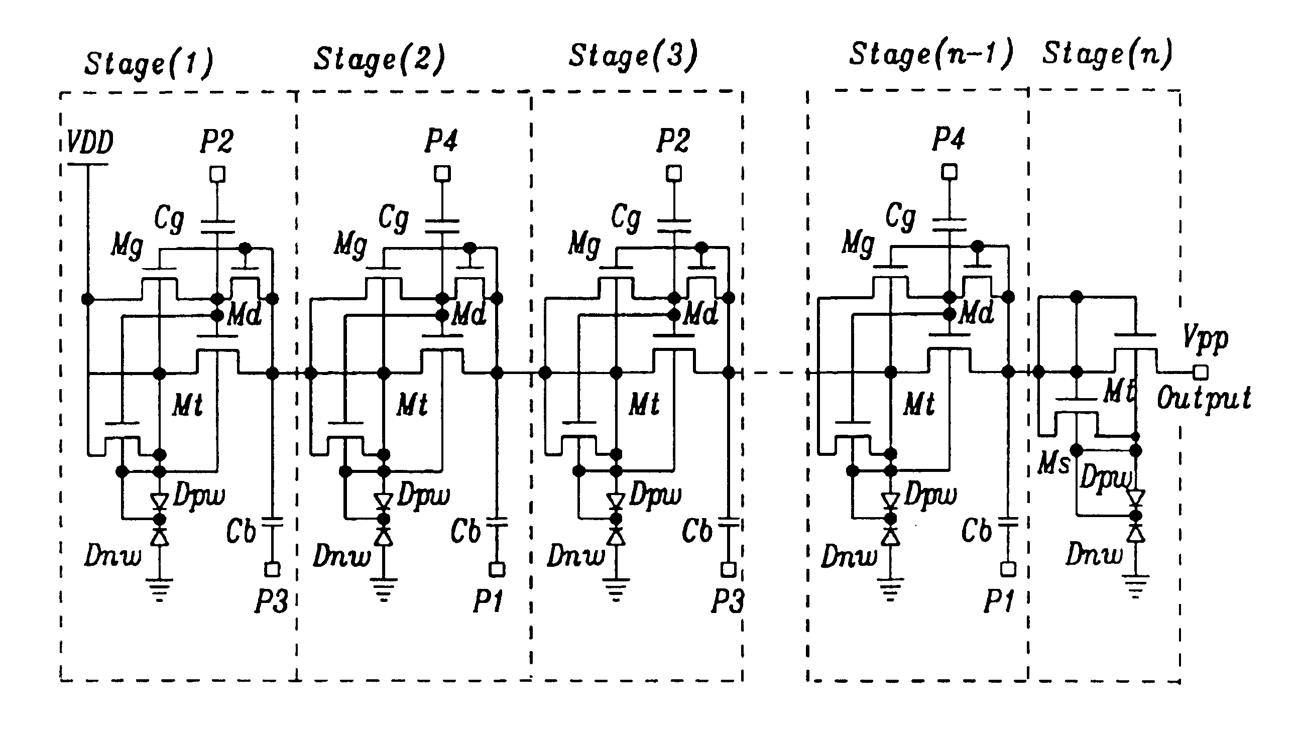
[0040]FIG. 7 shows a circuit diagram of the charge pump of the present invention where the negative effects of the triple well are reduced by the inclusion of the auxiliary MOSFET device Ms. Included in the circuit diagram are Dpw, the parasitic diode between the P-well and the deep N-well, and Dnw, the parasitic diode between the deep N-well and the P-substrate. Other, and less important, parasitic diodes and capacitances associated with MOS devices are not shown for ease of understanding of the circuit diagram. Pumping stages are connected in series from power supply VDD to the high voltage output Vpp. Each pumping stage is formed in its own P-well and deep N-well. The P-well acts as substrate region of the MOS devices in the pumping stage.

[0041]Each pumping stage includes three N-channel MOSFET devices, a charge transfer MOS device Mt, an auxiliary MOS device Mg to pre-charge a voltage on the gate of the charge transfer device Mt for increasing boost coupling effect, and an auxil...


PUM


Abstract

An improved charge pump circuit is provided using a triple-well structure where the charge pump circuit has a plurality of stages containing N-channel MOSFET devices in which each stage is contained in a P-well within a Deep N-well residing on a P-substrate. Each pump stage is formed in its own P-well and the pumping stages are serially connected from power supply source to the output terminal. Each pumping stage includes a charge transfer device, a first auxiliary device to precharge the gate of the charge transfer device with a voltage from the previous stage, and a second auxiliary device to switch coupling between the charge transfer device and its substrate region to reduce the body effect and increases the capacitive boosting effect. The multiple stages of circuitry are clocked from either a four-phase clock or a two-phase clock.

Description

[0001]This application claims priority to Provisional Patent Application Ser. No. 60 / 424,252, filed on Nov. 6, 2002, which is herein incorporated by referenceBACKGROUND OF THE INVENTION[0002]1. Field of Invention[0003]The present invention relates to integrated circuits and more specifically to charge pump circuits providing high output voltage and current at low power supply voltages.[0004]2. Description of Related Art[0005]A charge pump is widely used in semiconductor memories, and in particular non-volatile Electrically Erasable and Programmable Read Only Memories (EEPROM) where a voltage larger than the supplied chip voltages, such as 3.3V, 2.5V is generally required up to 10V or more. These high voltages are typically not available on the chip so they are generated from the low supplied voltage. These higher voltages are mainly required in such operations as programming and erase of a memory cell. As the power supply voltage to the chip is reduced down in the range of 1.2 to 1....

Claims


Application Information

Patent Timeline
Patent Type & Authority Patents(United States)
IPC IPC(8): H02M3/07H02M3/04
CPCH02M3/073
Inventor PARK, KI-TAEKOJI, SHIMENOOGURA, TOMOKO
Owner HALO LSI INC
Why Eureka
Try Eureka