Method for manufacturing semiconductor device, and method for manufacturing semiconductor module

a manufacturing method and technology for semiconductor devices, applied in semiconductor devices, semiconductor/solid-state device details, electrical devices, etc., can solve problems such as lowering reliability, slow etching speed, and lowering and achieve enhanced throughput of semiconductor devices and short time

Active Publication Date: 2005-07-12
SAMSUNG ELECTRONICS CO LTD
View PDF4 Cites 115 Cited by
  • Summary
  • Abstract
  • Description
  • Claims
  • Application Information

AI Technical Summary

Benefits of technology

[0020]As a result, the semiconductor substrate can be thinned down by spin etching, and through electrodes can be formed in the semiconductor substrate without harming the flatness of the non-etching surface. Also, the semiconductor substrate can be thinned down and the through electrodes can be exposed in a short time. For this reason, the through electrodes can be effectively formed without lowering the reliability of semiconductor devices, and the throughput of semiconductor devices can be enhanced. Also, a stacked layered structure of semiconductor substrates can be precisely composed.

Problems solved by technology

When the dry etching is used in this manner, the etching speed is slow, and therefore the throughput of semiconductor devices is lowered.
In this case, when the semiconductor substrate 51 is connected to another semiconductor substrate or a circuit substrate, tip portions of the semiconductor substrate 51 may come in contact with the other semiconductor substrate or the circuit substrate, which causes a problem of lowered reliability.

Method used


Image

  • Method for manufacturing semiconductor device, and method for manufacturing semiconductor module
  • Method for manufacturing semiconductor device, and method for manufacturing semiconductor module
  • Method for manufacturing semiconductor device, and method for manufacturing semiconductor module

Examples


Embodiment Construction

[0029]Hereafter, a method to manufacture a semiconductor device and a method to manufacture a semiconductor module will be described with reference to the accompanying figures.

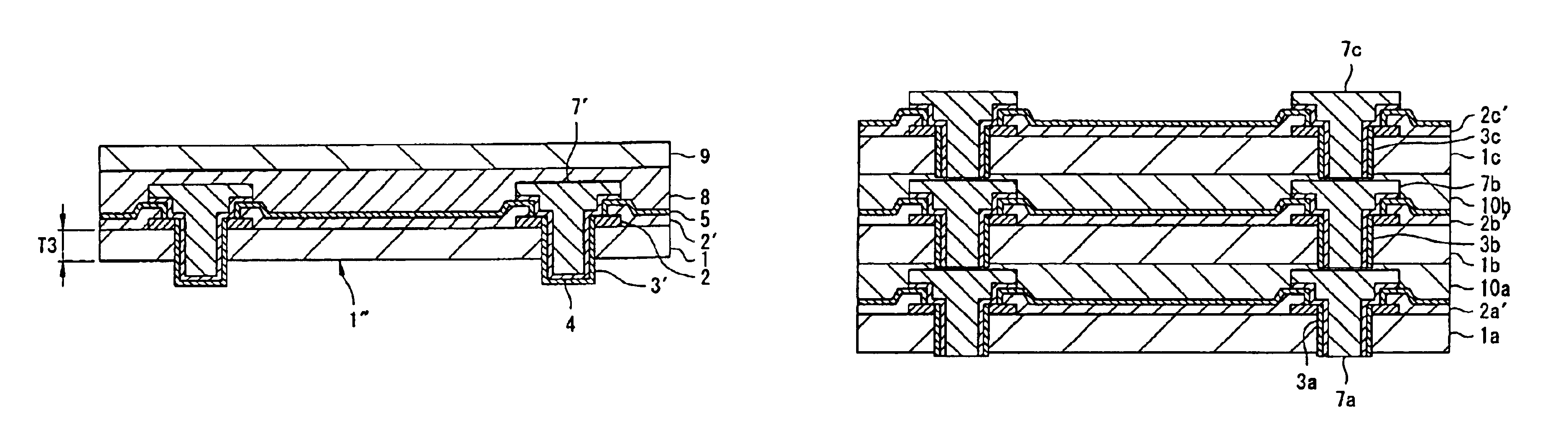
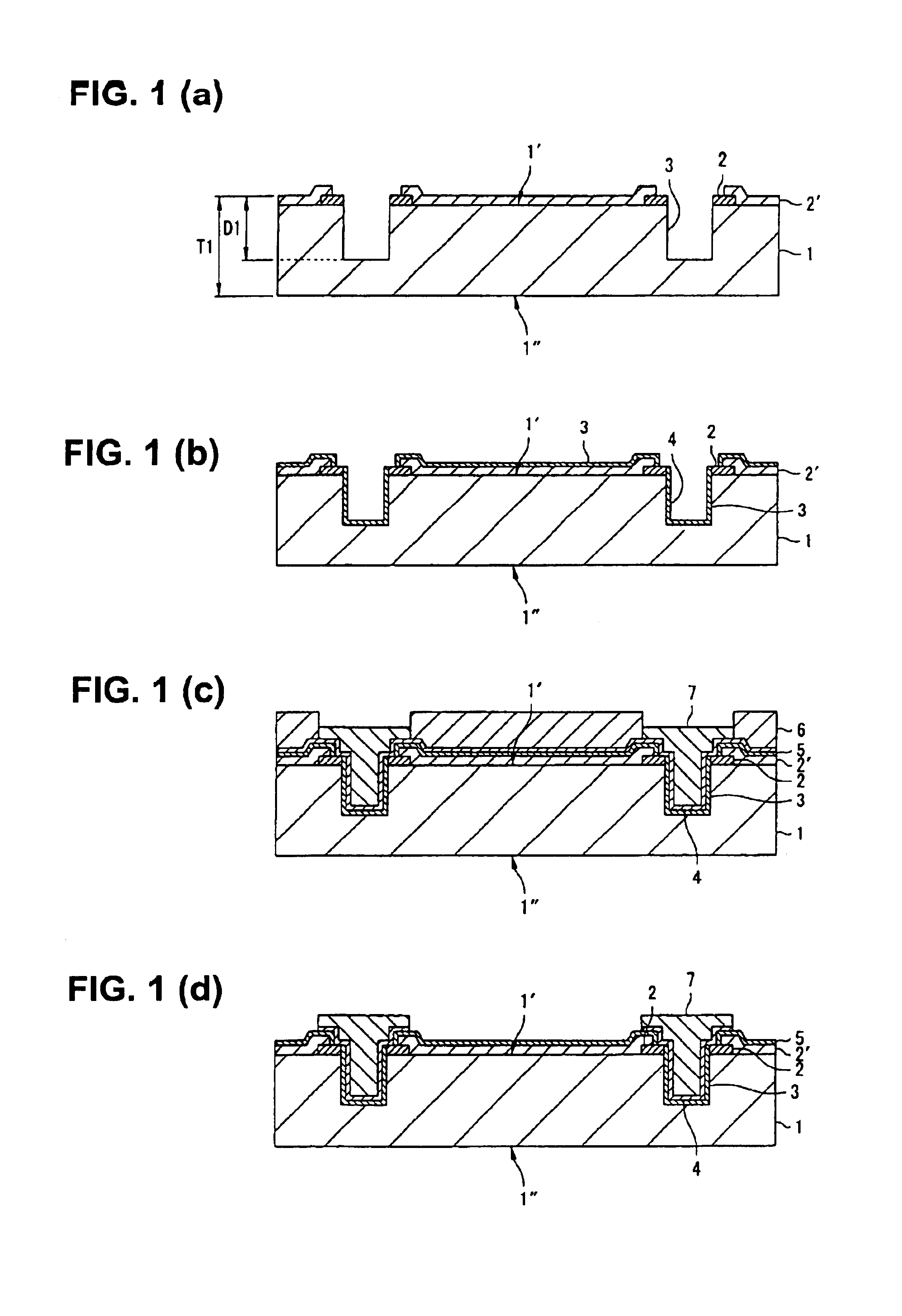
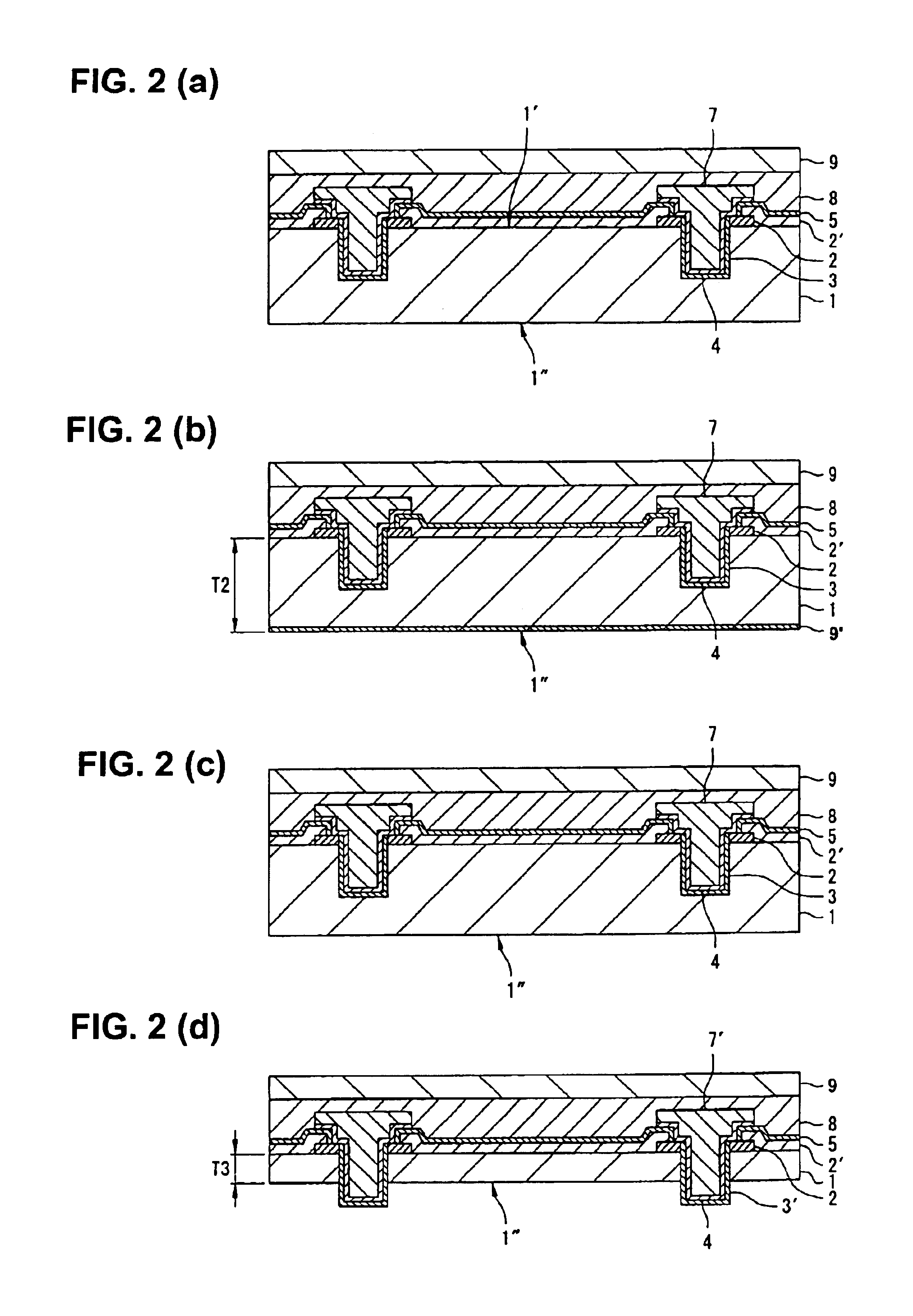
[0030]FIGS. 1 through 3 are cross-sectional views indicating a method to manufacture a semiconductor device in accordance with an exemplary embodiment of the present invention.

[0031]Referring to FIG. 1(a), electrode pads 2 are formed on a surface 1′ of a semiconductor substrate 1. The semiconductor substrate 1 may be a semiconductor wafer or a semiconductor chip that is one of segments of a semiconductor wafer. An integrated circuit is formed within the semiconductor substrate 1, and the electrode pads 2 are electrically connected to the integrated circuit. The semiconductor substrate 1 may have a dielectric film 2′ as a passivation film for the electrode pads 2 over the surface 1′. In this case, the passivation film may have opening sections at positions over the electrode pads 2.

[0032]Next, opening sections ...


PUM


Abstract

To form through electrodes effectively without deteriorating the quality of the through electrodes, a semiconductor substrate is spin etched at its back surface, thereby thinning down the semiconductor substrate, making opening sections penetrate the semiconductor substrate, and forming through holes in the semiconductor substrate. Tips of embedded electrodes are exposed out of the through holes in the semiconductor substrate, to form through electrodes.

Description

BACKGROUND OF THE INVENTION[0001]1. Field of Invention[0002]The present invention relates to methods to manufacture semiconductor devices and methods to manufacture semiconductor modules, and in particular, is applied to methods to form through electrodes in a substrate.[0003]2. Description of Related Art[0004]In related art semiconductor devices, to realize a stacked layered structure of semiconductor chips, there is a method in which through holes are formed in semiconductor substrates, and the semiconductor substrates are interconnected via through electrodes that are embedded in the through holes.[0005]FIGS. 8(a)-8(d) are cross-sectional views indicating a related art method to manufacture a semiconductor device.[0006]Referring to FIG. 8(a), pad electrodes 52 are formed on a surface 51′ of a semiconductor substrate 51. Opening sections 53 are formed through the pad electrodes 52 in the semiconductor substrate 51. Next, as indicated in FIGS. 8(b) and(c), dielectric films 54 are f...

Claims


Application Information

Patent Timeline
Patent Type & Authority Patents(United States)
IPC IPC(8): H01L25/065H01L21/44H01L21/46H01L21/02H01L21/304H01L21/3205H01L25/18H01L25/07H01L23/52H01L21/768H01L23/48
CPCH01L21/76898H01L23/481H01L25/0657H01L2224/16145H01L2225/06517H01L2225/06513H01L2225/06541H01L2225/06565H01L2924/00014H01L2224/05644H01L2224/05647H01L2224/05655H01L2224/05684H01L2224/05099
Inventor YAMAGUCHI, KOJI
Owner SAMSUNG ELECTRONICS CO LTD
Why Eureka
Try Eureka