Fluorescent lamp, fluorescent lamp unit, liquid crystal display device, and method of emitting light
- Summary
- Abstract
- Description
- Claims
- Application Information
AI Technical Summary
Benefits of technology
Problems solved by technology
Method used
Image

Examples
first embodiment
[0084]A flat panel fluorescent lamp according to a first embodiment and a liquid crystal display device which employs the flat panel fluorescent lamp as a back light will now be explained.
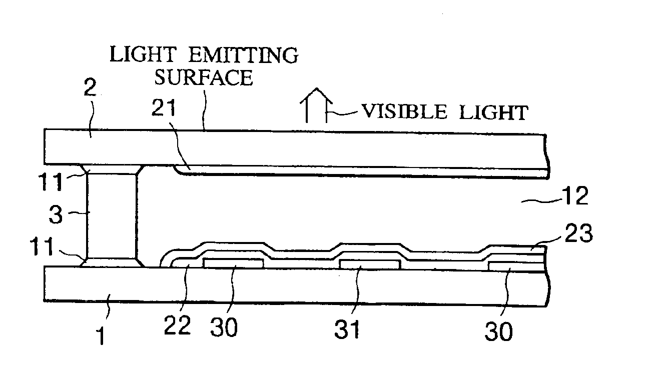
[0085]As shown in FIG. 4, this liquid crystal display device comprises a liquid crystal display panel 6 and a flat panel fluorescent lamp 20. The liquid crystal display panel 6 and the flat panel fluorescent lamp 20 are held by a front chassis (case) 7, a center chassis 8, and a rear chassis 9. A circuit substrate 10 is attached at the back surface of the rear chassis 9. An inverter circuit which generates a voltage for driving the flat panel fluorescent lamp 20 is loaded (provided) on the circuit substrate 10. A power source cable 13 for transmitting electrical power form the inverter circuit to the flat panel fluorescent lamp 20 is connected to the circuit substrate 10 and the fluorescent lamp 20.
[0086]FIG. 5 illustrates a cross sectional structure of the flat panel fluorescent lamp 20 in detail....
second embodiment
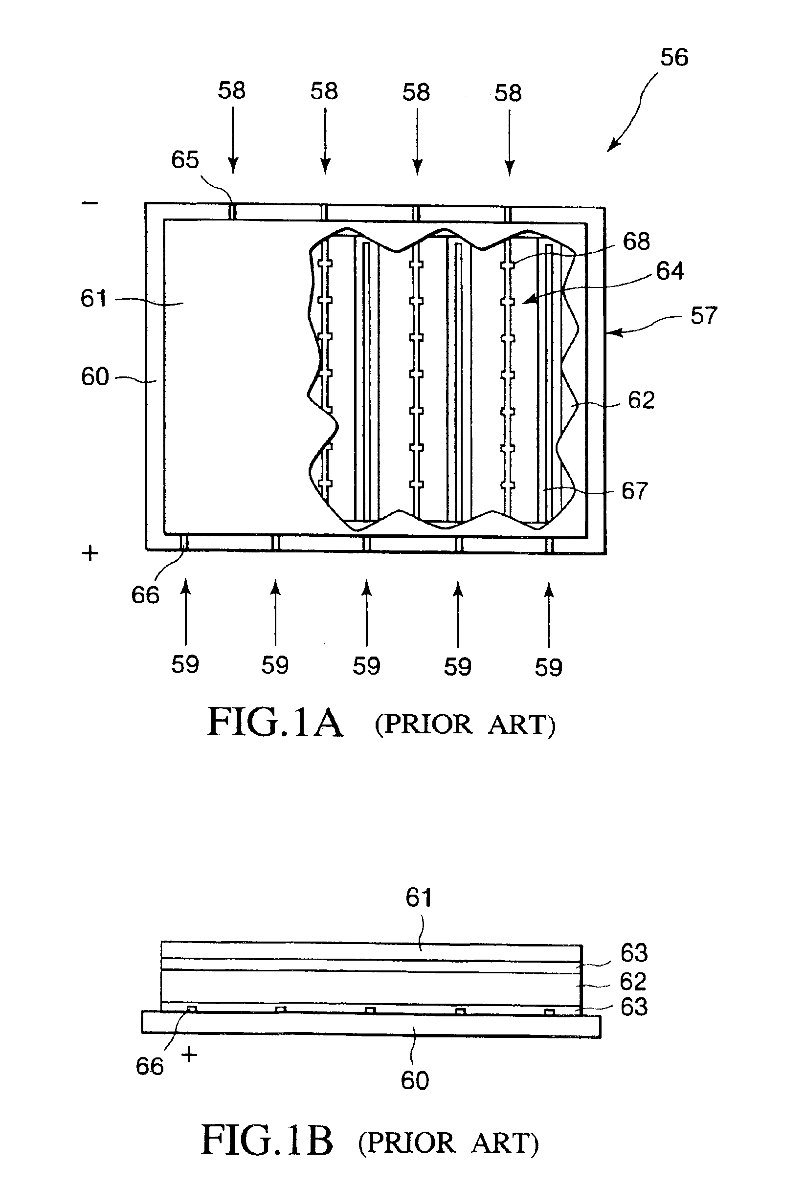
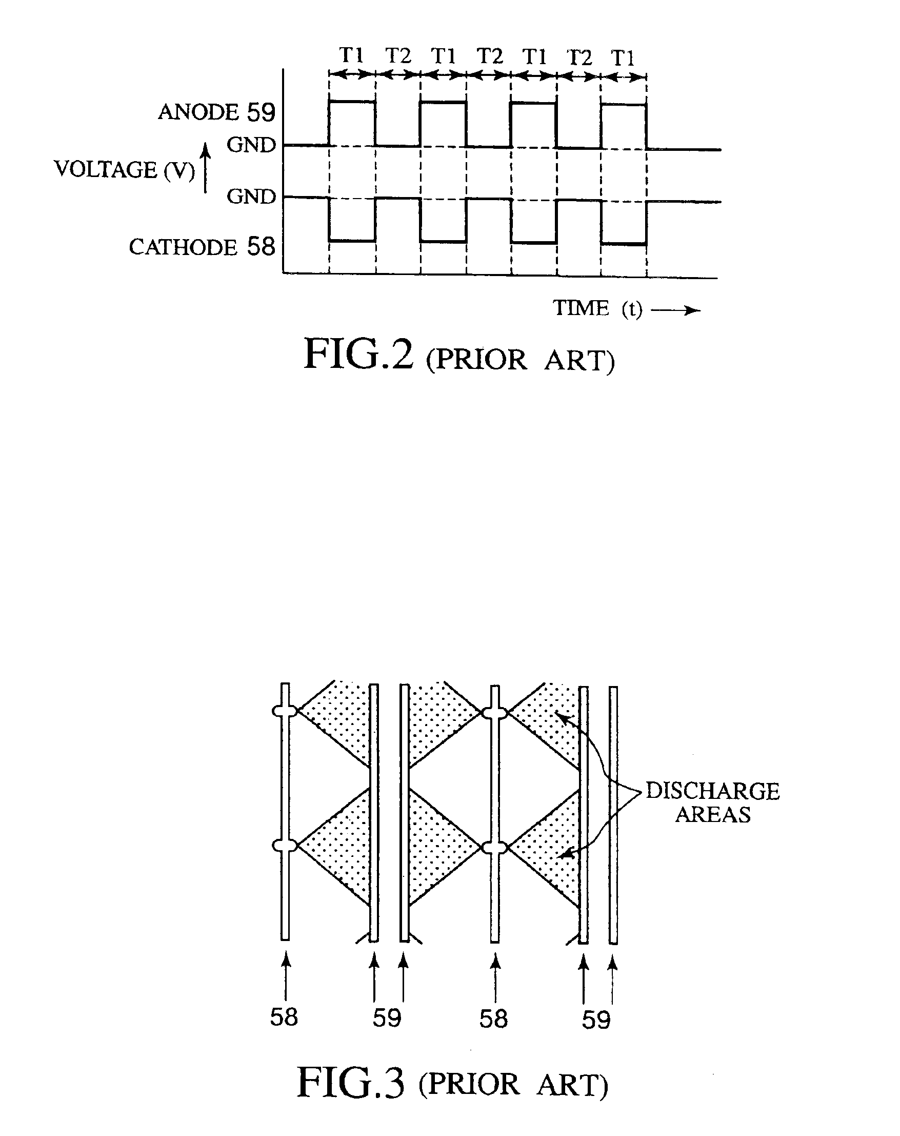
[0102]A flat panel fluorescent lamp 20 according to a second embodiment of the present invention will now be explained. As shown in FIG. 11, in the flat panel fluorescent lamp 20 according to the second embodiment, first electrodes 30 are placed on a lower substrate 1, and second electrodes 31 are placed on an upper substrate 2. The plan view of the arrangement of the electrodes as seen from above the flat panel fluorescent lamp 20 is the same as in case of the fluorescent lamp 20 of the first embodiment. Accordingly, during a period T1 in which a negative voltage is applied to the first electrodes 30 and a positive voltage is applied to the second electrodes 31, electric discharge is caused in a pattern shown in FIG. 8A or in FIG. 10A. During a period T2 in which a positive voltage is applied to the first electrodes 30 and a negative voltage is applied to the second electrodes 31, electric discharge is caused in a pattern shown in FIG. 8B or in FIG. 10B.
[0103]In the structure shown...
third embodiment
[0104]A flat panel fluorescent lamp according to a third embodiment of the present invention will now be explained. A difference between the flat panel fluorescent lamp according to the third embodiment and that of the first and second embodiments is that the fluorescent lamp of this embodiment has three groups of electrodes.
[0105]FIG. 12 shows a cross section of the flat panel fluorescent lamp of this embodiment. FIGS. 12A and 12B show arrangements of electrodes. As shown in FIG. 12A, first electrodes 30 and second electrodes 31 are alternately arranged on a lower substrate 1 almost in parallel. The first electrodes 30 are mutually connected and the second electrodes 31 a mutually connected. Third electrodes 32 are made of a transparent conductive material such as ITO, and arranged on an upper substrate 2 so as to face the second electrodes 31 as shown in FIG. 12B. The third electrodes 32 are mutually connected.
[0106]As shown in FIG. 12A, projections 24 are not provided to the firs...
PUM
 Abstract
Description
Claims
Application Information
 - Generate Ideas
- Intellectual Property
- Life Sciences
- Materials
- Tech Scout
- Unparalleled Data Quality
- Higher Quality Content
- 60% Fewer Hallucinations
Browse by: Latest US Patents, China's latest patents, Technical Efficacy Thesaurus, Application Domain, Technology Topic, Popular Technical Reports.
© 2025 PatSnap. All rights reserved.Legal|Privacy policy|Modern Slavery Act Transparency Statement|Sitemap|About US| Contact US: help@patsnap.com