Check patentability & draft patents in minutes with Patsnap Eureka AI!

One time programmable solid-state device

Inactive Publication Date: 2005-07-12
RE SECURED NETWORKS LLC
View PDF8 Cites 23 Cited by
  • Summary
  • Abstract
  • Description
  • Claims
  • Application Information

AI Technical Summary

Problems solved by technology

In the manufacture of conventional CCD and CMOS imaging devices, the re are often a number of defective photodetectors in each array.
These defective pixels often result in degraded picture quality from the solid-state imaging device.
There are several disadvantages to storing defective pixels in this manner.
First, utilizing an external memory chip adds extra steps and thus increases the assembly time of the device in which the memory chip is utilized (e.g., a digital camera, or a USB “universal-serial busperipheral).
Furthermore, the overall cost to manufacture the device is increased due to both the increased assembly time, and the requirement of an extra external memory chip on the PCB.
Finally, the need for an additional memory chip increases the number of external electrical connections and increases the complexity of the device and opportunities of malfunctions.

Method used


Image

  • One time programmable solid-state device
  • One time programmable solid-state device
  • One time programmable solid-state device

Examples


Embodiment Construction

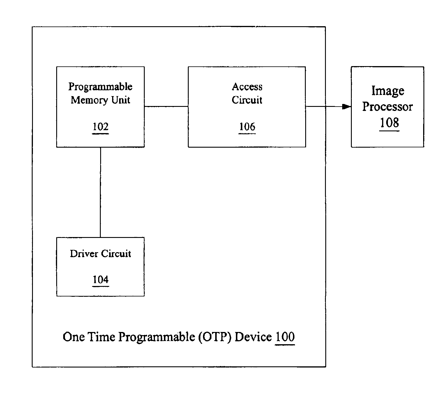
[0028]In FIG. 1, a one time programmable “OTP” device 100 is illustrated. The OTP device 100 typically includes a programmable memory unit 102, a driver circuit 104, and an access circuit 106. The OTP device 100 is embedded within the die of a solid-state (i.e., semiconductor) integrated circuit chip (“IC”), and is thus on the same substrate as the IC. The solid-state IC may be, for example, a solid-state imaging device (such as a CCD, CMOS or CID) utilized in a digital camera or an application-specific IC (ASIC) used in a USB peripheral.

[0029]As an example, in solid-state imaging device, it is typically necessary to identify bad (i.e., defective) pixels (i.e., photodetectors) in the photosensor (i.e., photosensitive imaging array) of the imaging device before image processing occurs so that the image processor may perform image correction to compensate for the defective pixels. To perform image correction during image processing, an image processor 108 may obtain the location of ea...


PUM


Abstract

A one time programmable solid-state device is provided such that the programmable solid-state device includes a programmable memory unit embedded in a die and a driver circuit that programs the programmable memory unit. The one time programmable solid-state device also includes an access circuit that enables access to the programmable memory unit. In an example operation when the one-time programmable solid-state is a solid-state image device, the one-time programmable solid-state device performs the process of identifying an address of a defective pixel in a photosensor having a plurality of pixels arranged in a two-dimensional array in the die and storing the address in the programmable memory unit that is embedded in the die of the solid-state imaging device.

Description

BACKGROUND OF THE INVENTION[0001]1. Technical Field[0002]This invention relates generally to programmable solid-state devices, and more particularly, to permanently programmable solid-state devices.[0003]2. Related Art[0004]Solid-state imaging devices (also referred to as image devices or imagers) have broad applications in many areas including commercial, consumer, industrial, medical, defense and scientific fields. Solid-state imaging devices convert a received image from an object into a signal indicative of the received image. Solid-state imaging devices are fabricated from semiconductor materials (such as silicon or gallium arsenide) and include photosensitive imaging arrays (photosensors) of light detecting picture elements, or pixels, (also known as photodetectors) interconnected to generate analog signals representative of the received image. Examples of solid-state imaging devices include charge coupled devices (CCD), photodiode arrays, charge injection devices (CID), hybri...

Claims


Application Information

Patent Timeline
IPC IPC(8): H04N9/64H04N5/367H04N5/369
CPCH04N5/367H04N25/68
Inventor TAY, HIOK-NAM
Owner RE SECURED NETWORKS LLC
Features
  • R&D
  • Intellectual Property
  • Life Sciences
  • Materials
  • Tech Scout
  • Unparalleled Data Quality
  • Higher Quality Content
  • 60% Fewer Hallucinations
Learn More