Semiconductor device manufacturing method and semiconductor device manufactured thereby

a semiconductor device and manufacturing method technology, applied in semiconductor devices, semiconductor/solid-state device details, electrical devices, etc., can solve the problems of increased manufacturing and manufacturing facilities, performance loss, and inability to apply the soldering of internal leads, and achieve the effect of high reliability and ease of working

Inactive Publication Date: 2005-07-19
KK TOSHIBA
View PDF10 Cites 30 Cited by
  • Summary
  • Abstract
  • Description
  • Claims
  • Application Information

AI Technical Summary

Benefits of technology

[0007]It is an object of the present invention to provide a method of connecting a semiconductor chip to external leads with ease of working and high reliability.
[0012]According to the present invention, the use of the inner lead frame allows an inner lead to be solder bonded to a small electrode, such as a gate electrode, simultaneously with a soldering process for die mounting. Thus, the manufacturing process is simplified. The need of a wire bonding process using costly gold wires is eliminated, simplifying the manufacturing facilities.
[0013]The application of the present invention to a multi-chip package in which two or more semiconductor chips are molded allows the parasitic inductance and wiring resistance associated with a printed wiring board to be reduced and the device performance to be increased. Also, the packing density can be increased.

Problems solved by technology

With three-terminal devices, such as power MOS FETs, which handle relatively high current, soldering connection is desirable; however, since a gate electrode formed on a chip are very small in comparison with a source electrode, soldering of internal leads can not be applied because of poor position precision.
However, this method results in the increased cost of manufacture and manufacturing facility because different materials which involve different surface finishes for electrodes are used for the gate electrode and the source electrode.
With this approach, parasitic capacitance and resistance are associated with wiring, which may result in loss in performance.

Method used


Image

  • Semiconductor device manufacturing method and semiconductor device manufactured thereby
  • Semiconductor device manufacturing method and semiconductor device manufactured thereby
  • Semiconductor device manufacturing method and semiconductor device manufactured thereby

Examples


first embodiment

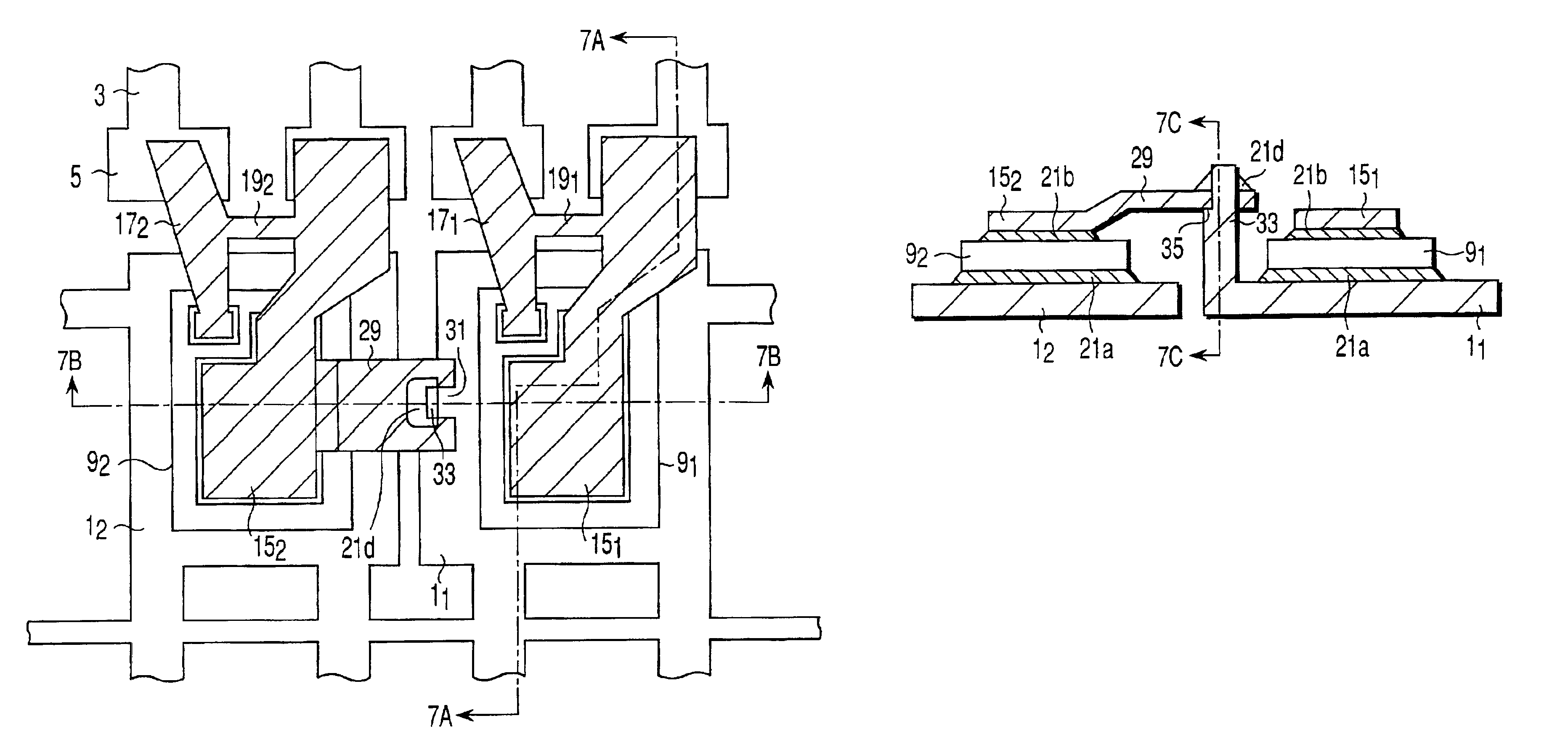
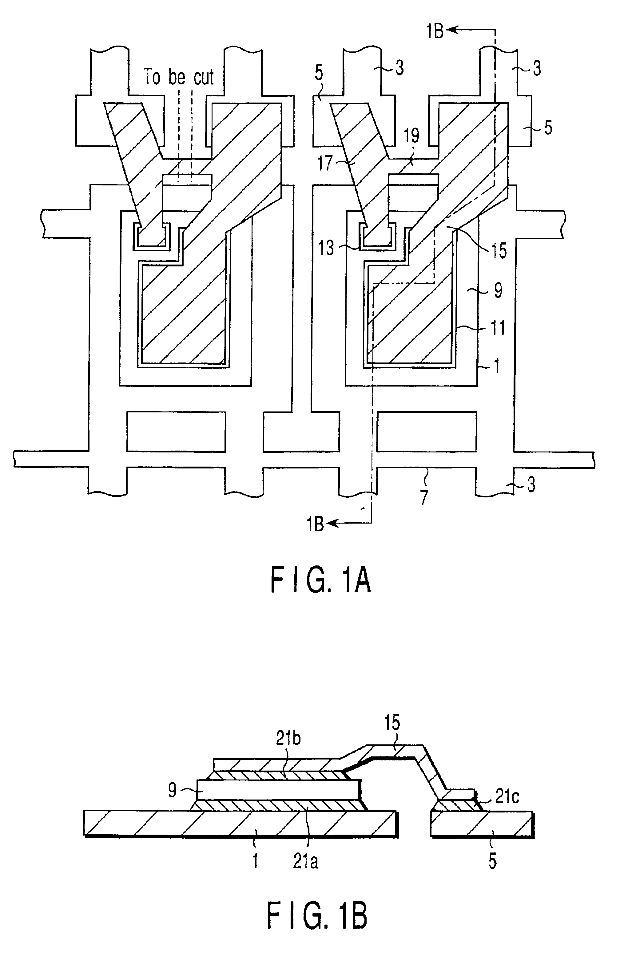
[0028]A semiconductor device manufacturing method according to the present invention will be described with reference to FIGS. 1A and 1B. FIG. 1A is a plan view illustrating the configuration in which a semiconductor chip is mounted on a lead frame and electrodes on the top of the semiconductor chip are electrically connected to external leads of the lead frame through inner leads, and FIG. 1B is a sectional view taken along line 1B—1B of FIG. 1A.

[0029]In FIGS. 1A and 1B, reference numeral 1 denotes a die pad in the lead frame, 3 denotes an external lead of the lead frame, 5 denotes an inner lead connecting pad formed integrally with the external lead 3, and 7 denotes a tie bar adapted to form a well-known plastic seal lead frame, which is hereinafter referred to as the external lead frame for distinction from an internal lead frame to be described later.

[0030]To the die pad 1 of the external lead frame is attached a semiconductor chip 9 by a bonding material 21a which may be solder...

second embodiment

[0043][Second Embodiment]

[0044]A second embodiment of the present invention is basically the same as the first embodiment except for the shape of the die pads.

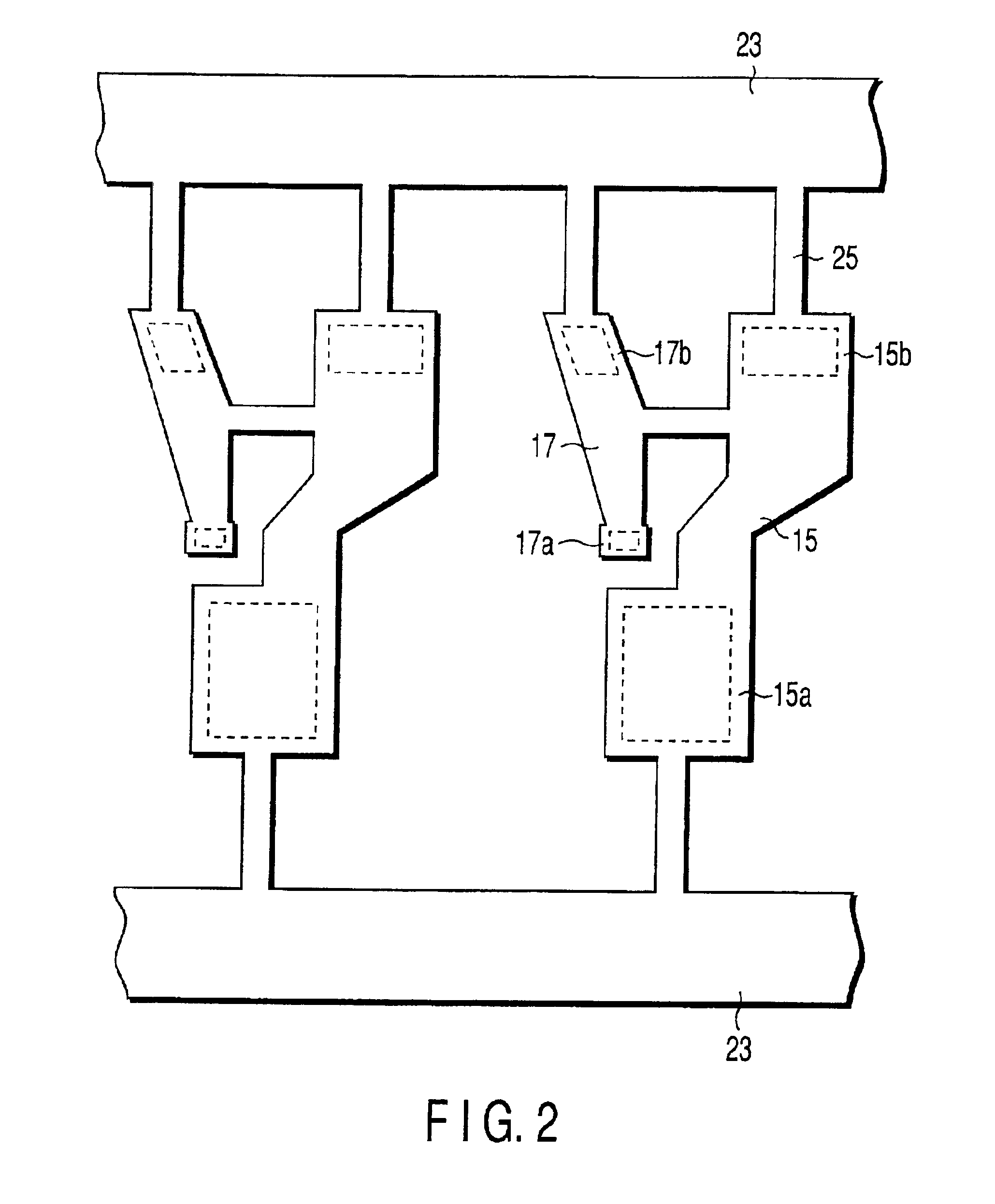
[0045]FIG. 3 is a plan view illustrating the inner connections in a semiconductor device according to the second embodiment of the present invention. Like reference numerals are used to denote corresponding parts to those in FIG. 1A and descriptions thereof are omitted. The same is true of still other embodiments.

[0046]The second embodiment is characterized in that, as shown in FIG. 3, the die pad 1a is formed with a notch 26 in its portion close to the tie bar 19 of the inner lead frame. The notch allows easy cutting of the tie bar.

third embodiment

[0047][Third Embodiment]

[0048]FIG. 4A is a plan view of an inner lead according to a third embodiment of the present invention and FIG. 4B is an enlarged section view of the tie bar taken along line 4B—4B of FIG. 4A. In the second embodiment, as shown in FIG. 4B, the cutting portion 27 of the tie bar 19a is set smaller in thickness than the inner lead, thereby allowing easy cutting of the tie bar. For example, the thickness of the inner lead is set to 0.3 mm and the thickness of the cutting portion is set to 0.15 mm.


PUM


Abstract

A method of manufacturing a semiconductor device involves mounting a semiconductor chip, formed on top with a main electrode and a subelectrode smaller in area than the main electrode, on a die pad of an external lead frame through a first bonding material, mounting an inner lead frame in which plural inner leads for connecting the main electrode and the subelectrode on the chip to corresponding connecting pads of the external lead frame are joined together by a tie bar on the chip and the external lead frame through a second bonding material, heating the first and second bonding materials simultaneously for electrically connecting and fixing the chip to the die pad and the inner leads to the electrodes on the chip and the connecting pads of the external lead frame, and cutting the tie bar to separate the inner lead frame into the plural inner leads.

Description

CROSS-REFERENCE TO RELATED APPLICATIONS[0001]This application is based upon and claims the benefit of priority from the prior Japanese Patent Application No. 2000-287385, filed Sep. 21, 2000, the entire contents of which are incorporated herein by reference.BACKGROUND OF THE INVENTION[0002]The present invention relates to a method of manufacturing semiconductor devices and a semiconductor device manufactured by the method.[0003]With the recent spread of portable electronic devices, the demand has increased for scaling down the dimensions of, reducing the weight of, and enhancing the performance of semiconductor packages. Heretofore, electrodes on top of semiconductor chips are connected to external leads by means of wire bonding. Two-terminal devices, such as diodes, are connected through internal leads to external leads by means of soldering.[0004]With three-terminal devices, such as power MOS FETs, which handle relatively high current, soldering connection is desirable; however, s...

Claims


Application Information

Patent Timeline
Patent Type & Authority Patents(United States)
IPC IPC(8): H01L21/60H01L23/495H01L21/02H01L23/48H01L25/10H01L25/11
CPCH01L23/49562H01L24/33H01L24/32H01L24/36H01L24/40H01L24/41H01L24/83H01L24/97H01L25/115H01L2924/12032H01L2924/1306H01L2924/014H01L2924/01006H01L2224/32245H01L2224/8319H01L2224/83801H01L2224/97H01L2924/01004H01L2924/01005H01L2924/01013H01L2924/01029H01L2924/01033H01L2924/01079H01L2924/01082H01L2924/0781H01L2924/13091H01L2924/19041H01L2924/19042H01L2924/19043H01L2924/30105H01L2924/30107H01L2224/83H01L2924/00H01L2224/40095H01L2224/40245H01L2224/4103H01L24/38H01L2224/77272H01L2224/45144H01L2224/0603H01L2224/84801H01L2224/8385H01L2924/00014H01L2224/8485H01L2224/84385H01L2224/37013H01L24/84H01L2224/37099H01L2224/73221H01L21/60
Inventor UCHIDA, SHOTARO
Owner KK TOSHIBA
Why Eureka
Try Eureka