Fuse detection circuit

a detection circuit and fuse technology, applied in logic circuit coupling/interface arrangement, pulse technique, instruments, etc., can solve the problem of not being able to draw up to 100% of the laser device capacity, and achieve the effect of reducing the layout area

Inactive Publication Date: 2005-07-19
LAPIS SEMICON CO LTD
View PDF4 Cites 30 Cited by
  • Summary
  • Abstract
  • Description
  • Claims
  • Application Information

AI Technical Summary

Benefits of technology

[0007]According to such a circuit configuration, even when only some of the fuse has been blown, the cutting out of the fuse can be judged by making a comparison of the presence or absence of the fuse cutout with the reference resistance. Accordingly, it is possible to use fuse dimensions in the vicinity of the limit capability of a laser device and thereby reduce the area of the fuse.
[0009]According to the circuit having such a configuration, since the transistors N6 and N7 are turned off after the fuse has been judged to be blown, through currents at a resistive element section and a non-cutout fuse section can be avoided.
[0011]According to such a circuit configuration, an effect can be obtained that the present fuse detection circuit normally operates even when, for example, a power supply voltage VCC is a low voltage such as 1.0V. Also an effect can be obtained that since the present fuse detection circuit can be composed of a small number of elements, a layout area can be reduced.

Problems solved by technology

However, the aforementioned dimension determining method has a problem that the capability of the laser device has not been drawn Up to 100%.
Since there may be a case wherein when the dimensions are set in accordance with the capability of the laser device, only some of the fuse is blown due to variations in process, the conventional detection circuit is accompanied by a problem that both the opening and short-circuiting of the fuse are not detected so that a logic output becomes indefinite, thus causing a malfunction.

Method used


Image

  • Fuse detection circuit
  • Fuse detection circuit
  • Fuse detection circuit

Examples


first embodiment

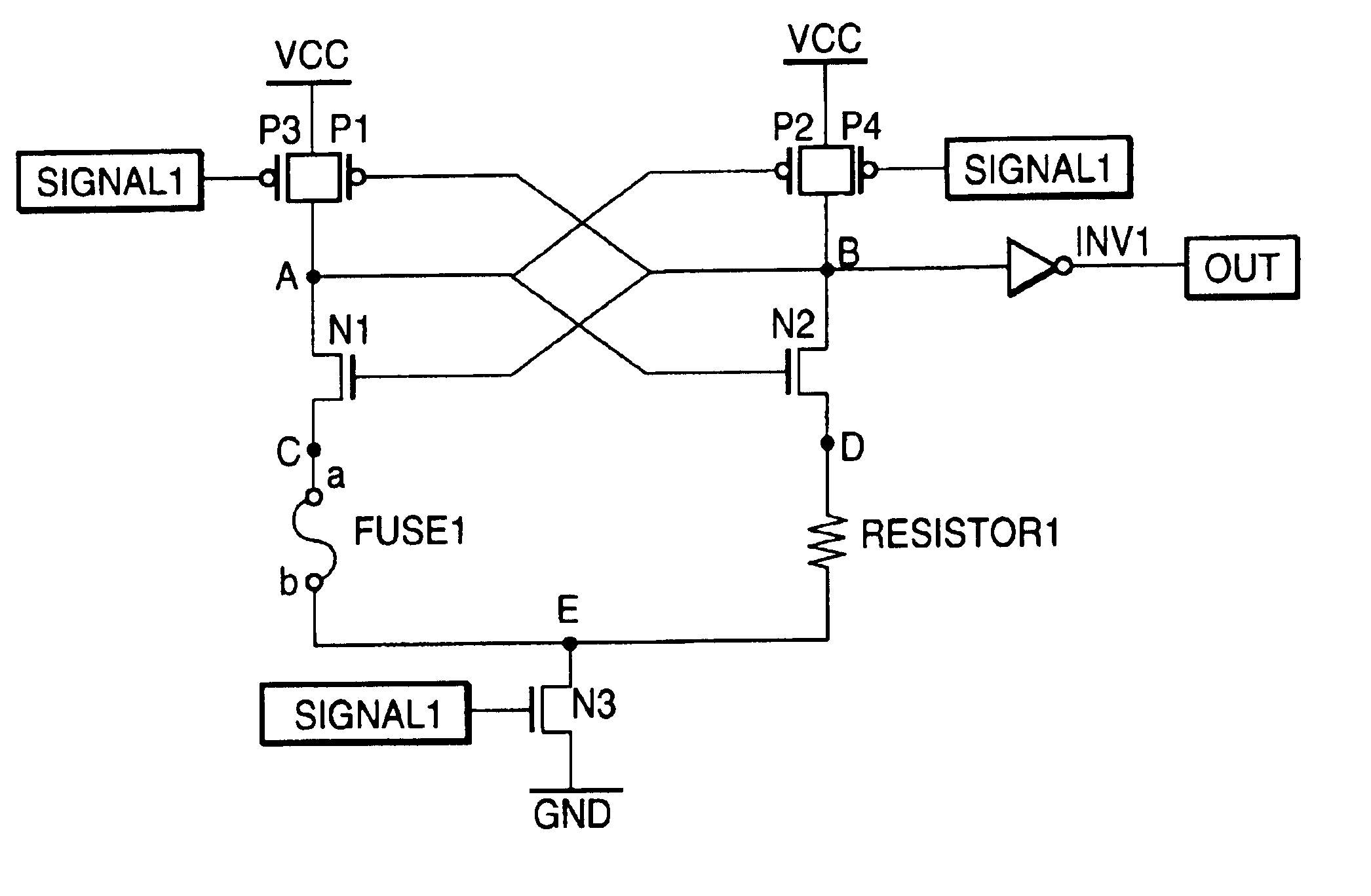
[0017]FIG. 1 is a circuit diagram of a fuse detection circuit showing a first embodiment of the present invention. The fuse detection circuit comprises a fuse element (fuse 1), a resistive element (resistor 1) used as the reference, PMOS transistors (P1 through P4), NMOS transistors (N1 through N5), and a CMOS inverter (INV1).

[0018]One terminal b of the fuse 1 is connected to the drain of the transistor N4, and the other terminal a of the fuse 1 is connected to the drain of the transistor N1, the drain of the transistor P1, and the drain of the transistor P3, i.e., a node A.

[0019]The source of the transistor N4 is connected to a reference potential (e.g., ground potential) GND, the source of the transistor N1 is connected to the drain (node C) of the transistor N3, the sources of the transistors P1 and P3 are respectively connected to a power supply voltage VCC, and the source of the transistor N3 is connected to the reference potential GND.

[0020]One terminal of the resistor 1 is co...

second embodiment

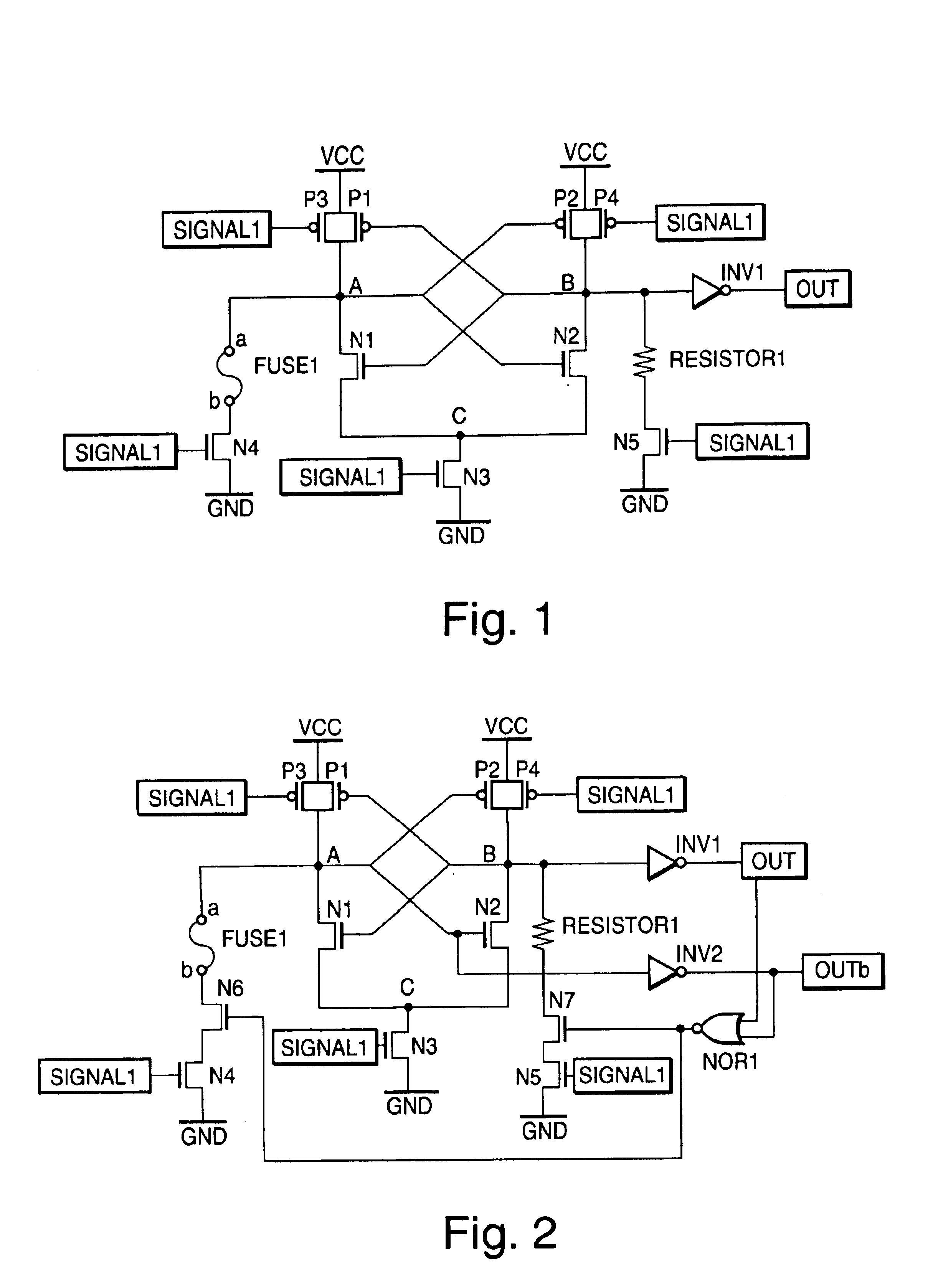
[0029]FIG. 2 is a circuit diagram showing a second embodiment of the present invention. The present embodiment comprises a fuse element (fuse 1), a resistive element (resistor 1) used as the reference, PMOS transistors (P1 through P4), NMOS transistors (N1 through N7), CMOS inverters (INV1 and INV2), and a CMOS NOR gate (NOR1).

[0030]One terminal b of the fuse 1 is connected to the drain of the transistor N6, and the other terminal a of the fuse 1 is connected to the drain of the transistor N1, the drain of the transistor P1, and the drain of the transistor P3, i.e., a node A.

[0031]The source of the transistor N6 is connected to the drain of the transistor N4, the source of which is connected to a reference potential GND. The source of the transistor N1 is connected to the drain (node C) of the transistor N3, the sources of the transistors P1 and P3 are respectively connected to a power supply voltage VCC, and the source of the transistor N3 is connected to the reference potential GN...

third embodiment

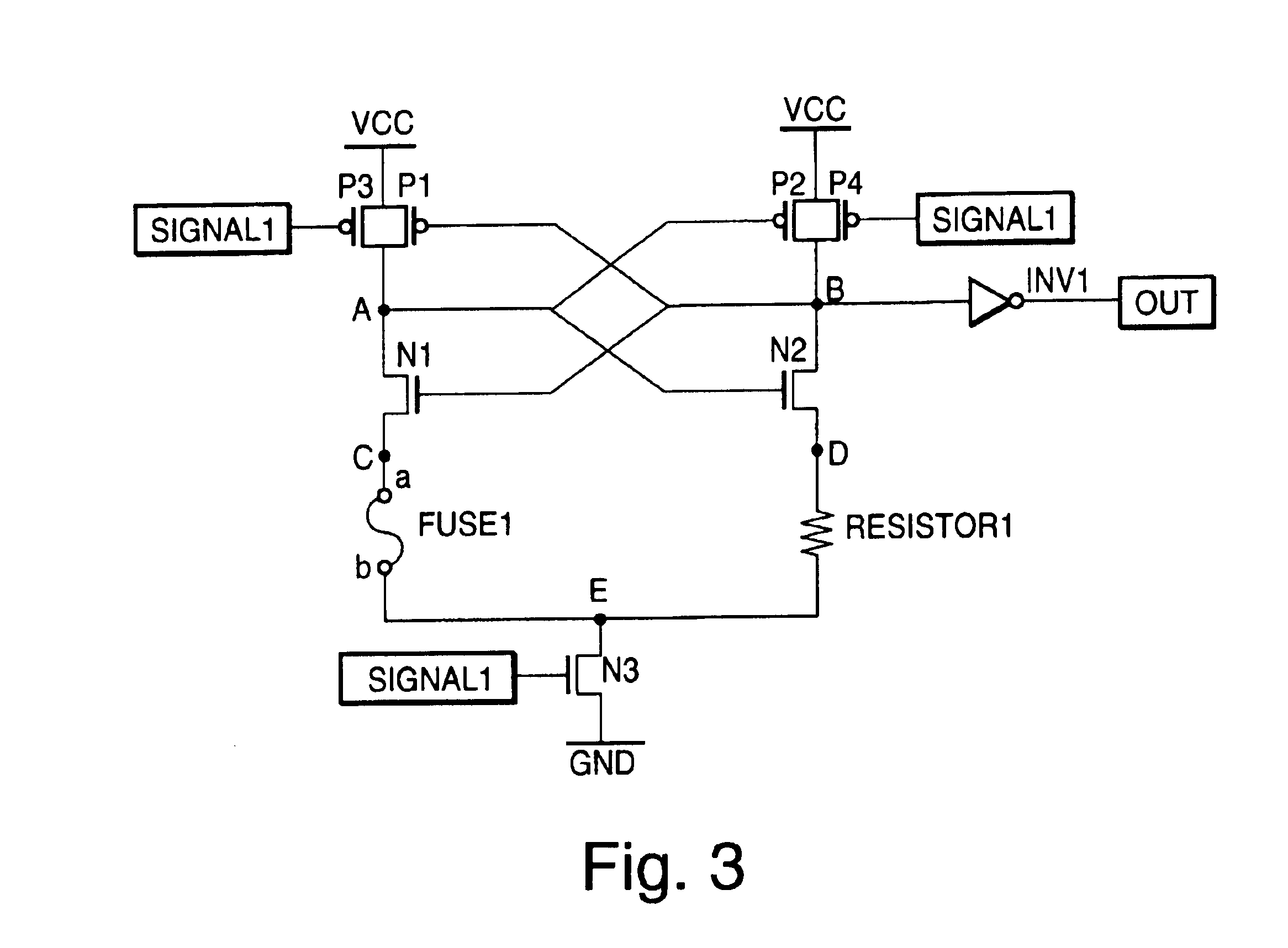
[0043]FIG. 3 is a circuit diagram showing a third embodiment of the present invention, which comprises a fuse element (fuse 1), a resistive element (resistor 1) used as the reference, PMOS transistors (P1 through P4), NMOS transistors (N1 through N3), and a CMOS inverter (INV1).

[0044]One terminal a of the fuse 1 is connected to the source (node C) of the transistor N1, and the other terminal b of the fuse 1 is connected to the drain (node E) of the transistor N3. The drain of the transistor N1 is connected to the drains of the transistors P1 and P3, i.e., a node A, the source of the transistor N3 is connected to a reference potential GND, and the sources of the transistors P1 and P3 are connected to a power supply voltage VCC.

[0045]One terminal of the resistor 1 is connected to the source (node D) of the transistor N2, and the other terminal of the resistor 1 is connected to the node E. The drain of the transistor N2 is connected to the drains of the transistors P2 and P4, i.e., a n...


PUM


Abstract

There is provided a fuse detection circuit comprising a first inverter circuit comprising a PMOS transistor (P2) and an NMOS transistor (N2) having gates connected in common and connected to the first node (A); a second inverter circuit comprising a PMOS transistor (P1) and an NMOS transistor (N1) having gates connected in common and connected to the second node (B); and a third NMOS transistor (N3) having a drain and source connected between the third node (C) and the ground potential, and a gate connected with the control signal, wherein the control signal is set to a predetermined level in an initial state to precharge the node (A),(B) and thereafter a molten state of a fuse is detected in accordance with a potential level of the second node (B) at a change in the level of the control signal.

Description

BACKGROUND OF THE INVENTION[0001]1. Field of the Invention[0002]The present invention relates to a semiconductor device, and particularly to a fuse detection circuit.[0003]2. Description of the Related Art[0004]In general, a method of, using a fuse composed of a conductor, storing the status of the fuse according to whether it is cut out by laser, and reading its stored status by a detection circuit, has been used for a fuse detection circuit. The dimensions of the fuse are determined according to the accuracy of a laser device. There is a tendency to allow the fuse to assume a 10% cuttable setting (field-proven dimensions) with a view toward realizing stable high yields.[0005]However, the aforementioned dimension determining method has a problem that the capability of the laser device has not been drawn Up to 100%. Since there may be a case wherein when the dimensions are set in accordance with the capability of the laser device, only some of the fuse is blown due to variations in ...

Claims


Application Information

Patent Timeline
Patent Type & Authority Patents(United States)
IPC IPC(8): G11C29/38G11C17/14G11C29/04G11C17/18G11C29/02H01L27/04H01L21/82H01L21/822H03K19/0175
CPCG11C17/18G11C29/02G11C29/027G11C29/38
Inventor KUROKI, KOJI
Owner LAPIS SEMICON CO LTD
Why Eureka
Try Eureka