
Device for flat illumination of an object field

a technology for objects and objects, applied in waveguides, photometry, electrotherapy, etc., can solve the problems of affecting image quality and image quality, and achieve the effect of reducing interference and ensuring the effect of uniformity

Inactive Publication Date: 2005-08-02
CARL ZEISS MICROELECTRONICS SYST
View PDF7 Cites 27 Cited by
  • Summary
  • Abstract
  • Description
  • Claims
  • Application Information

AI Technical Summary

Benefits of technology

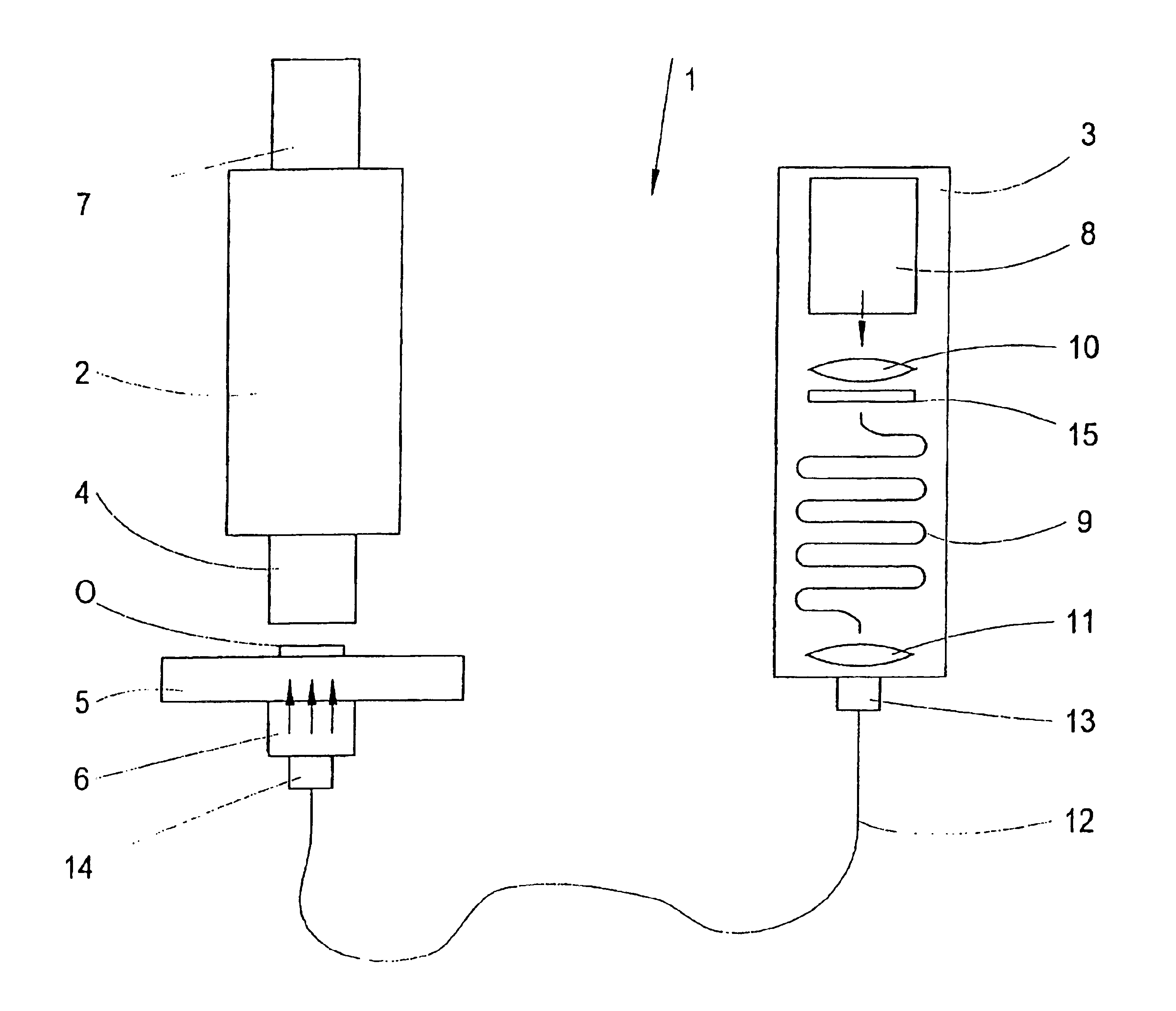
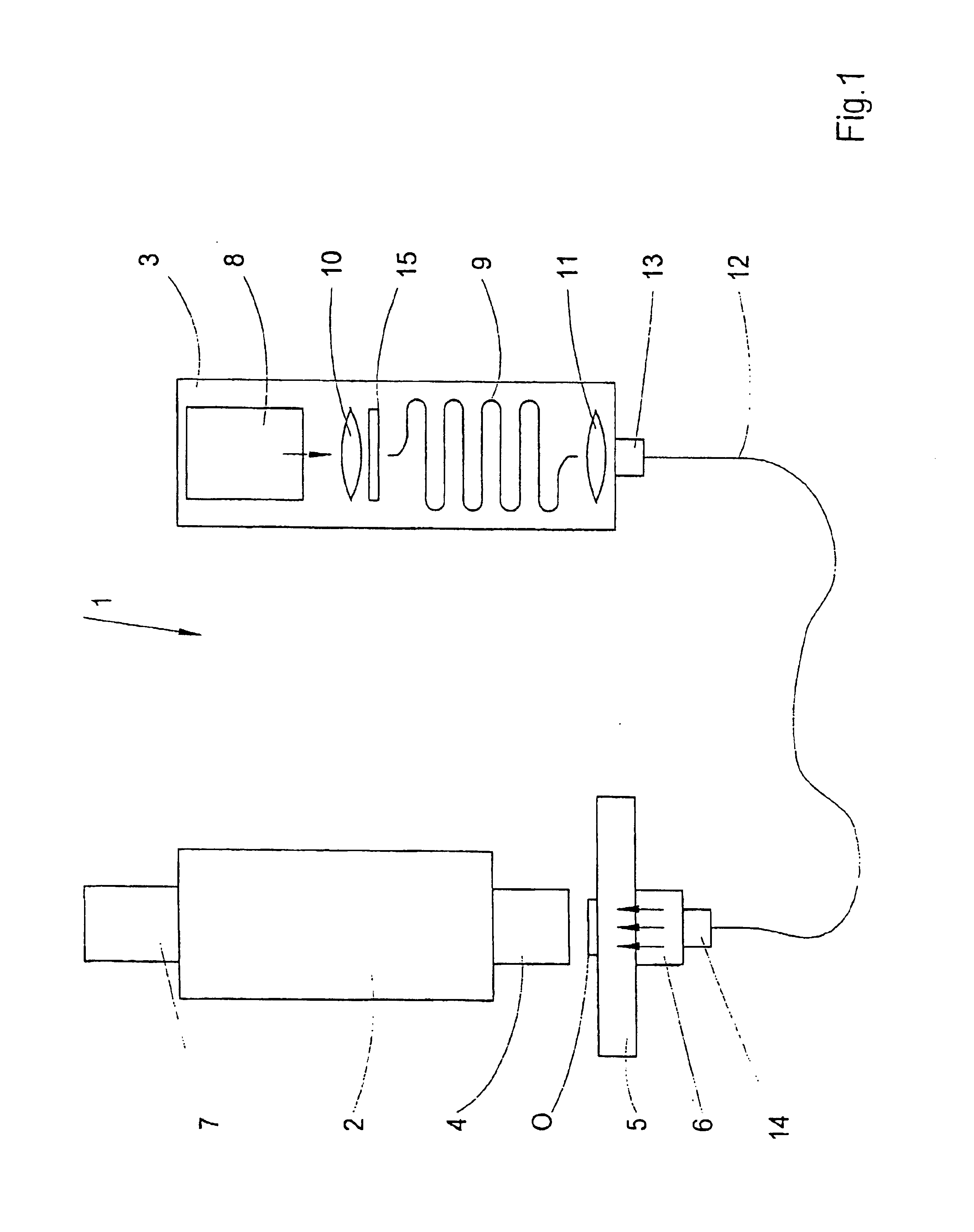
[0011]The effect achieved in this way is similar to that of a rotating scatter disk. In contrast to the rotating scatter disk, however, the inventive solution is a static system offering particularly extensive protection against interference due to the absence of moving components. In addition, the drive device and associated controls required for a rotating scatter disk are dispensed with.
[0012]The light-conducting cable can be arranged in a flexible manner with no special restrictions with respect to its position, so that greater compactness can also be achieved in instrument construction in contrast to a scatter disk.
[0017]To further improve and homogenize the illumination, one or more rotating scatter disks can also be arranged in front of and / or behind the light-conducting cable.

Problems solved by technology

To this extent, the problem with using laser light sources for generating the illumination light is that the intensity of the light is unevenly distributed within the beam cross section, which has a disadvantageous effect on image quality.
Other variations in the brightness of the illumination which disadvantageously affect the image quality and, therefore, the results of evaluation are caused by low-frequency amplitude modulations or coherent noise (speckle) in coherent light sources.

Method used


Image

  • Device for flat illumination of an object field
  • Device for flat illumination of an object field

Examples


Embodiment Construction

[0025]The microscope 1, which is constructed in this case as a microlithography simulation microscope by way of example, is outfitted with an observation device 2 and an illumination device 3. In this way, for example, masks for semiconductor or wafer fabrication as well as other objects can be examined.

[0026]The observation device 2 comprises an objective 4 which is directed toward a movable table 5 with a receptacle for an object O to be examined. Further, illumination optics 6 are provided for uniform illumination of a flat object field on the object O. In the present embodiment example, illumination is provided based on the principle of transmitted light. However, it is also possible to illuminate and examine the object O based on incident light.

[0027]The observation device 2 shown here is constructed for scanning a plurality of object points in the object field. Image information obtained in this way is recorded in a video camera 7 connected to the observation device 2. However...


PUM


Abstract

The invention is directed to a device for flat illumination of an object field in an optical instrument and to an optical instrument with a device of this kind. Optical instruments of this type are, for example, microscopes, including microlithography simulation microscopes in which a flat illumination, i.e., illumination extending beyond a singular object point, of the object to be examined is required. The device comprises a laser light source and a light-conducting cable with at least one optical fiber through which the light from the laser light source is guided to the object field. The optical fiber is constructed and dimensioned in such a way that the intensity of the illumination light within the cross section of the optical fiber becomes increasingly more uniform along the path from the input-side end to the output-side end, and the illumination light is directed from the output-side end of the optical fiber to the object with substantially homogeneous intensity distribution.

Description

CROSS-REFERENCE TO RELATED APPLICATIONS[0001]This application claims priority of PCT application No. PCT / EP02 / 07039, filed Jun. 26, 2002 and German application No. 101 30 821.3, filed Jun. 26, 2001, the complete disclosures of which are incorporated herein by reference.BACKGROUND OF THE INVENTION[0002]a) Field of the Invention[0003]The invention is directed to a device for flat illumination of an object field in an optical instrument and to an optical instrument with a device of this kind. Optical instruments of this type are, for example, microscopes, including microlithography simulation microscopes in which a flat illumination, i.e., illumination extending beyond a singular object point, of the object to be examined is required.[0004]b) Description of the Related Art[0005]In instruments of the type mentioned above, the homogeneity of the illumination of the object field is particularly important as regards the quality of the recorded images of the object field. To this extent, th...

Claims


Application Information

Patent Timeline
Patent Type & Authority Patents(United States)
IPC IPC(8): G02B21/06G02B6/00G02B21/16
CPCG02B21/06Y10S385/901
Inventor ENGEL, THOMASHARNISCH, WOLFGANGHEISE, JUERGEN
Owner CARL ZEISS MICROELECTRONICS SYST
Learn More