
Semiconductor component and method of manufacture

Active Publication Date: 2005-08-09
ADVANCED MICRO DEVICES INC
View PDF16 Cites 24 Cited by
  • Summary
  • Abstract
  • Description
  • Claims
  • Application Information

AI Technical Summary

Benefits of technology

[0011]In accordance with another aspect, the present invention comprises a method for reducing electromigration and stress migration in a semiconductor component. A damascene structure over a lower electrically conductive level is fabricated, wherein the damascene structure includes a dielectric material having a major surface and an opening extending into the dielectric material. The opening and a portion of the major surface are lined with a barrier layer to form a barrier-lined opening. The barrier-lined opening is filled with metal to form a metal-filled barrier-lined opening, which is then recessed so that an exposed surface of the metal-filled barrier-lined opening is below the major surface of the dielectric material. A capping layer is formed on the exposed surface of the metal-filled barrier-lined opening.

Problems solved by technology

As a result, the gate delays have been decreased to the point that speed is now primarily limited by the propagation delay of the metallization system used to interconnect the semiconductor devices with each other and with elements external to the semiconductor component.
A drawback to leaving the top surface unlined is that when current is being conducted through these structures voids are created by electromigration and stress migration.
These voids increase the resistance of the metallization system and degrade the performance of the semiconductor component.

Method used


Image

  • Semiconductor component and method of manufacture
  • Semiconductor component and method of manufacture
  • Semiconductor component and method of manufacture

Examples


Embodiment Construction

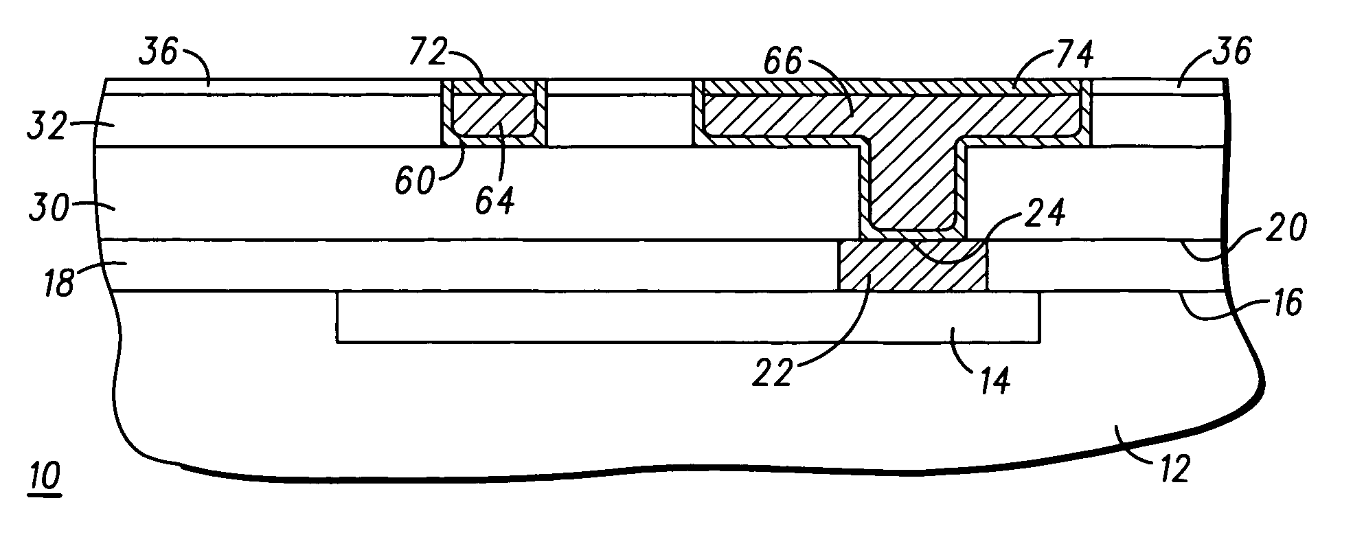
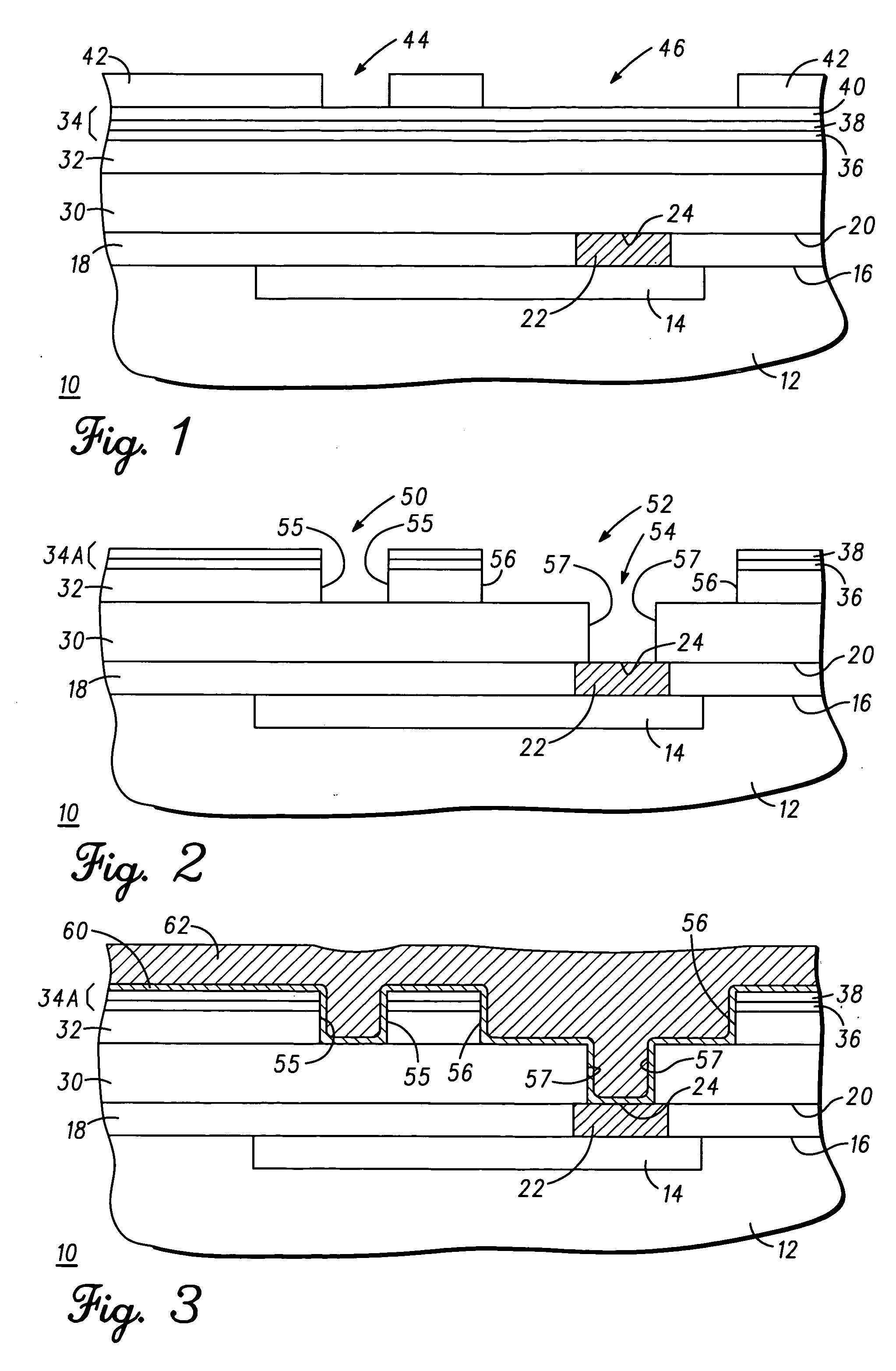
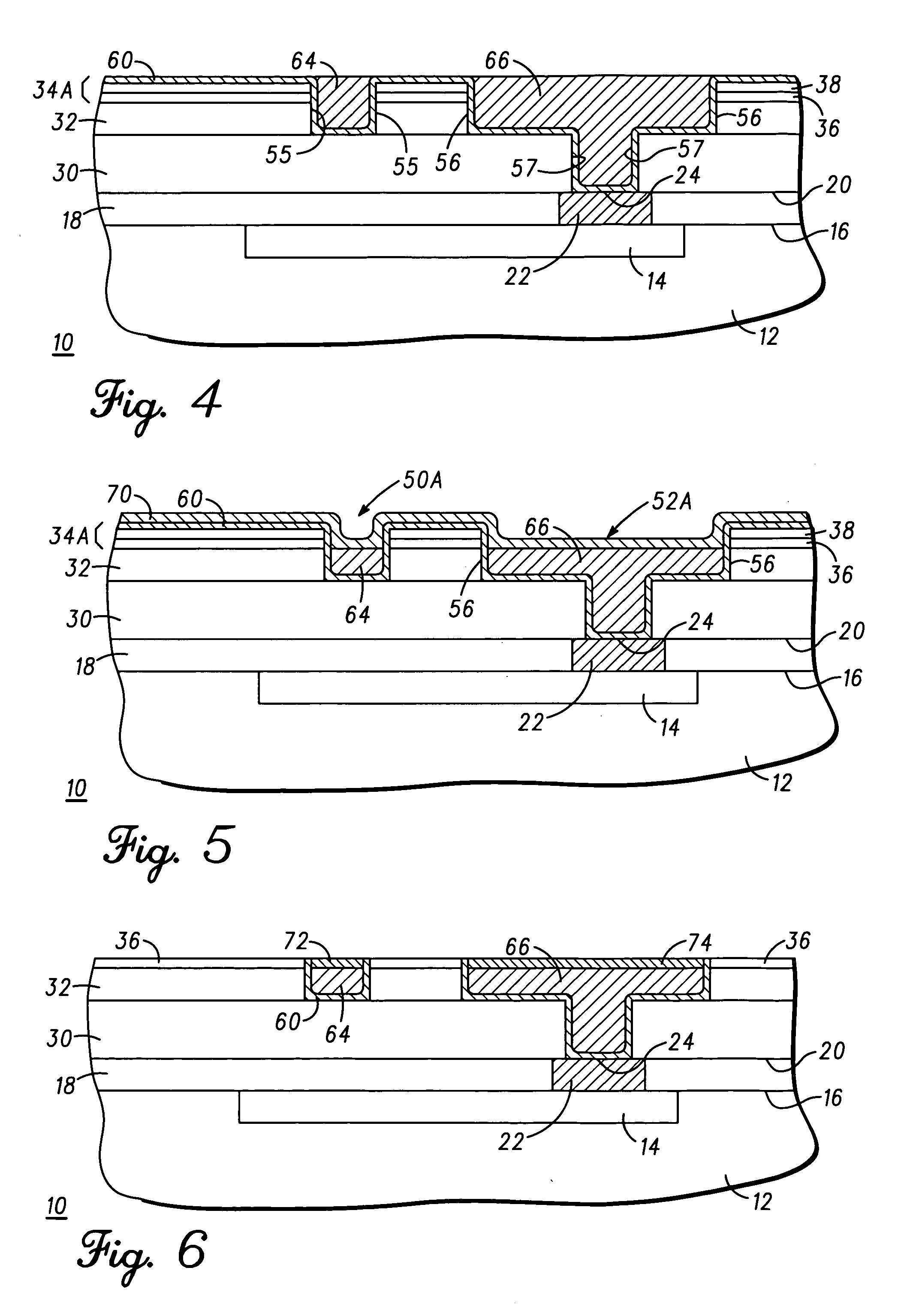
[0015]Generally, the present invention provides a semiconductor component having a multi-layer interconnect structure and a method for reducing electromigration and stress migration of a metal such as copper in the multi-layer interconnect structure. In accordance with one aspect of the present invention, a barrier layer is used to constrain the movement of copper atoms in the copper lines that make up the interconnect structure. The interconnect structure is manufactured using, for example, a damascene process, by forming a via in a dielectric stack comprising an insulating layer having an anti-reflective coating (ARC) layer disposed thereon. The via is lined with a barrier layer and then filled with copper. The copper is planarized (or polished) and recessed to form recessed copper-filled vias. A capping layer is formed in and over the recessed portions. The capping layer is made of a harder metal than copper and, while allowing the flow of current, prevents migration of the coppe...


PUM


Abstract

A semiconductor component and a method for manufacturing the semiconductor component that mitigates electromigration and stress migration in a metallization system of the semiconductor component. A hardmask is formed over a dielectric layer and an opening is etched through the hardmask and into the dielectric layer. The opening is lined with a barrier layer and filled with an electrically conductive material. The electrically conductive material is planarized, where the planarization process stops on the barrier layer. Following planarization, the electrically conductive material is recessed using either an over-polishing process with highly selective copper slurry or a wet etching process to partially re-open the filled metal-filled trench or via. The recess process is performed such that the exposed portion of the electrically conductive material is below the dielectric layer. A capping layer is then deposited on both the dielectric portion and the exposed metal interconnect portion of the electrically conductive material.

Description

FIELD OF THE INVENTION[0001]The present invention relates, in general, to a metallization system suitable for use in a semiconductor component and, more particularly, to a semiconductor component having a metallization system capable of mitigating electromigration and stress migration, to a method for manufacturing the semiconductor component, and to a method for mitigating electromigration and stress migration.BACKGROUND OF THE INVENTION[0002]Semiconductor component manufacturers are constantly striving to increase the speeds of their components. Because a semiconductor component, such as a microprocessor, contains up to a billion transistors or devices, the focus for increasing speed has been to decrease gate delays of the semiconductor devices that make up the semiconductor component. As a result, the gate delays have been decreased to the point that speed is now primarily limited by the propagation delay of the metallization system used to interconnect the semiconductor devices ...

Claims


Application Information

Patent Timeline
IPC IPC(8): H01L21/70H01L21/8238H01L21/768H01L23/532
CPCH01L23/5329H01L21/76811H01L21/76835H01L21/7684H01L21/76849H01L23/53238H01L2924/0002H01L2924/00
Inventor SAHOTA, KASHMIR S.MARTIN, JEREMYHUANG, RICHARD J.XIE, JAMES J.
Owner ADVANCED MICRO DEVICES INC
Learn More