Low power low voltage differential signaling driver

a low-power, differential signaling technology, applied in the field of data signaling, can solve the problems of increasing the die area requirement of the embodiment of fig. 3 and the supply voltage headroom of the stacked p-channel transistor, and reducing the power consumption of the p-channel transistor. the effect of reducing the requirement of power consumption

Active Publication Date: 2005-08-09
XILINX INC
View PDF3 Cites 38 Cited by
  • Summary
  • Abstract
  • Description
  • Claims
  • Application Information

AI Technical Summary

Benefits of technology

[0007]The low power low voltage differential signaling (LVDS) driver of the present invention substantially meets these needs and others. In one embodiment, a low power LVDS driver includes a load current source, first and second input transistors, first and second switchable current sources, and a switchable current source control module. The load current source is operably coupled to provide a load current. The first input transistor includes a gate, a drain, and a source, wherein the source of the first input transistor is coupled to the load current source, and wherein the gate of the first input transistor is operably coupled to receive a first leg of a differential input signal. The second input transistor includes a gate, a drain, and a source, wherein the source of the second input transistor is coupled to the load current source, wherein the gate of the second input transistor is operably coupled to receive a second leg of the differential input signal, and wherein the drains of the first and second input transistors provide an output of the low power LVDS driver. The first switchable current source is operably coupled to the drain of the first input transistor and to a power supply source, wherein, when enabled, the first switchable current source provides a first current to the drain of the second input transistor via at least one of a source termination and a load. The second switchable current source is operably coupled to the drain of the second input transistor and to the power suppl...

Problems solved by technology

But when the supply voltage drops below 2 volts (e.g., 1.8 volts for 0.18 micron CMOS technology), the LVDS driver of FIG. 2 does not have enough supply voltage headroom for the stacked P-channel transistors.
With a 1.8 volt supply, there is only 0.23 volts of ...

Method used


Image

  • Low power low voltage differential signaling driver
  • Low power low voltage differential signaling driver
  • Low power low voltage differential signaling driver

Examples


Embodiment Construction

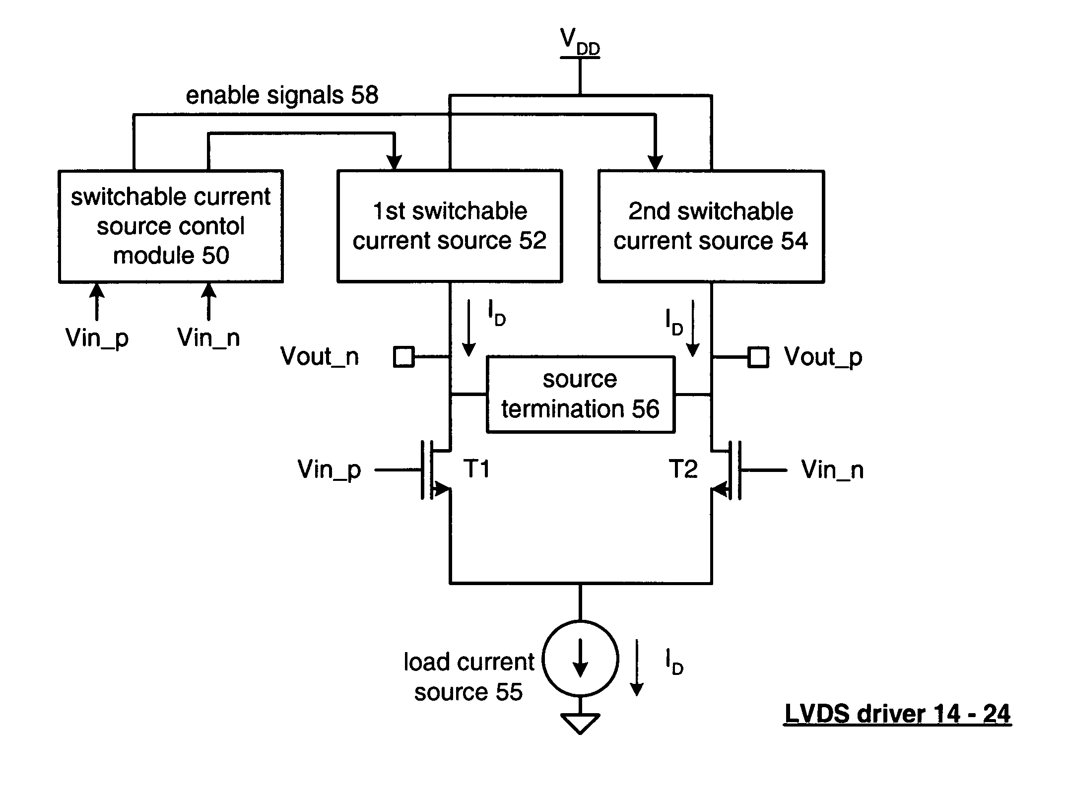
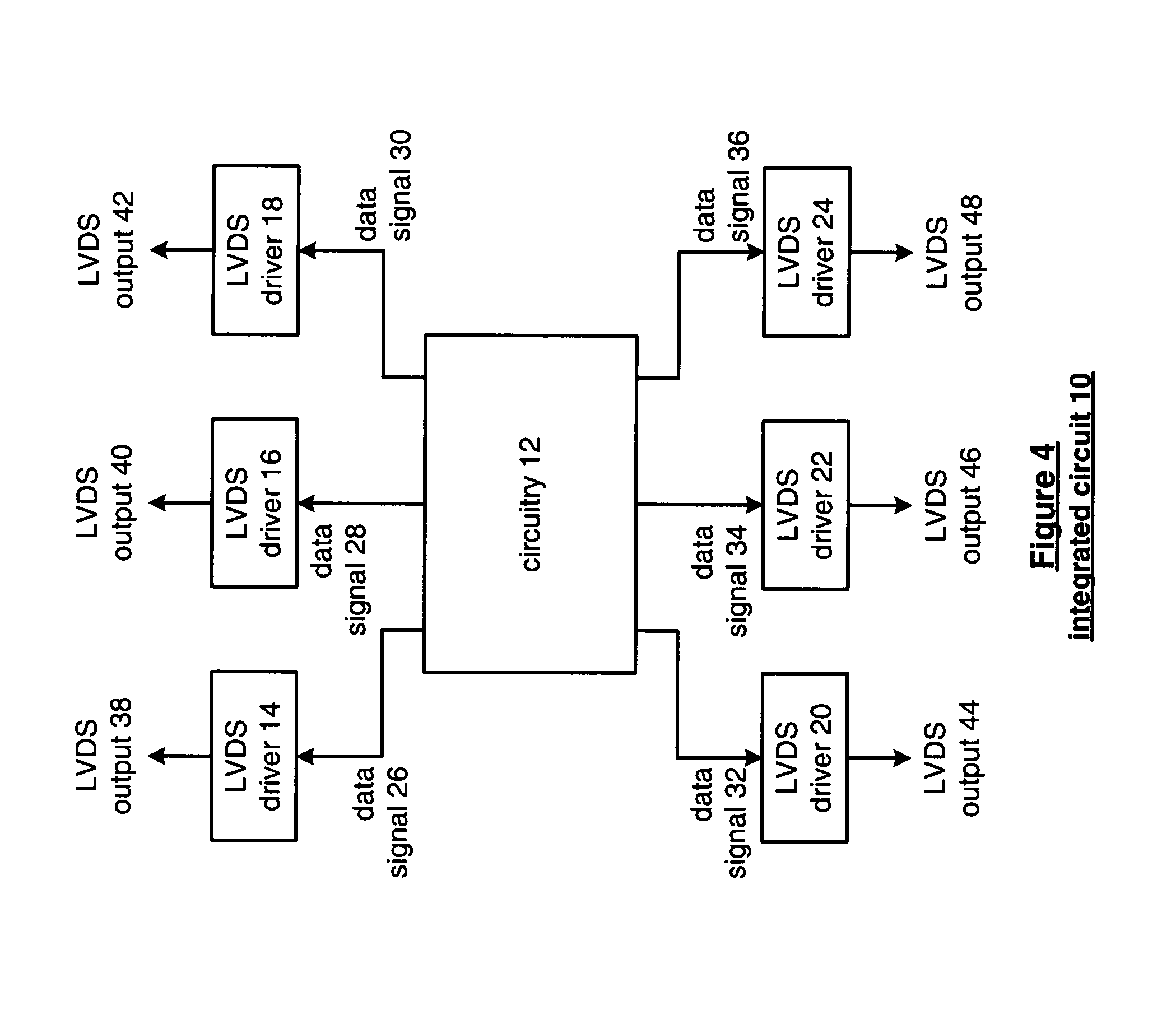
[0019]FIG. 4 is a schematic block diagram of an integrated circuit 10 that includes circuitry 12 and a plurality of a low voltage differential signaling (LVDS) drivers 14–24. The circuitry 12 may be analog circuitry, digital circuitry, processing circuitry and / or memory that produce a plurality of data signals 26–36. The data signals may be analog or digital signals. For example, circuitry 12 may be a programmable logic device (such as a field programmable gate array or a complex programmable logic device) comprising programmable logic blocks, programmable I / O blocks, and a programmable interconnect structure. In some embodiments, the programmable I / O blocks may include one or more LVDS drivers, such as drivers 14–24. If the data signals 26–36 are digital signals, they may represent a serial data stream having a data rate in the hundreds of megabits-per-second to gigabits-per-second. Each of the LVDS drivers 14–24 receives a corresponding data signal 26–36 and produce a correspondin...


PUM


Abstract

A low power LVDS driver includes a switchable current module, a source termination circuit, a transistor section, and a load current source. The switchable current module is operably coupled to produce a first current when a differential input signal is in a first state and to produce a second current when the differential input signal is in a second state. The source termination circuit is operably coupled in parallel with a load. The transistor section is operably coupled to receive the first and second currents from the switchable current module via at least one of the source termination circuit and the load, wherein the transistor section produces an LVDS output signal based on the first and second currents, the differential input signal, and the source termination circuit. The load current source is operably coupled to sink the first and second currents from the transistor section.

Description

FIELD OF THE INVENTION[0001]This invention relates generally to data signaling and more particularly to low voltage differential signaling.BACKGROUND OF THE INVENTION[0002]As is known, low voltage differential signaling (LVDS) is a standardized data transmission format that is widely used for serial data transmissions. Such LVDS formatting is generally illustrated in FIG. 1. As shown in FIG. 1, a differential signal is centered about a common mode voltage of 1.25 volts. The magnitude of the differential signal is 0.4 volts. As such, with respect to ground, the LVDS signal varies in magnitude from 1.05 volts to 1.45 volts.[0003]One common embodiment of an LVDS driver is illustrated in FIG. 2. As shown in FIG. 2, the LVDS driver includes a P-channel current source, two P-channel input transistors, two N-channel input transistors and an N-channel current source. In addition, the LVDS driver may include impedance matching resistors to provide a desired output impedance, for example the ...

Claims


Application Information

Patent Timeline
IPC IPC(8): H03K17/687
CPCH03K17/6872
Inventor CHEN, MINGDENGNIX, MICHAEL A.
Owner XILINX INC
Why Eureka
Try Eureka