Semiconductor device and method for manufacturing the same

a technology of semiconductor devices and semiconductors, applied in semiconductor devices, semiconductor/solid-state device details, electrical apparatus, etc., can solve the problems of reducing reliability, difficult to realize a thickness of about 100 m or less essentially, and the device itself is also expensive, so as to achieve uniform spacing and improve reliability.

Inactive Publication Date: 2005-08-16
RENESAS ELECTRONICS CORP
View PDF19 Cites 84 Cited by
  • Summary
  • Abstract
  • Description
  • Claims
  • Application Information

AI Technical Summary

Benefits of technology

[0019]In view of the above, it is an object of the present invention to provide a semiconductor device in which a plurality of semiconductor chips is stacked in layers and sealed in a package and which can be improved in reliability and thinned, and a method for manufacturing the same.
[0065]With the above configurations, an upper-part semiconductor chip is stacked via a plurality of spacers on a lower-part semiconductor chip in layers, thus enabling preserving a uniform spacing between the upper-part and lower-part semiconductor chips.
[0066]Furthermore, it is possible to form spacers via which an upper-part semiconductor chip is stacked on a lower-part semiconductor chip with a uniform spacing preserved therebetween, using a potting method, a screen printing method, or a non-contact type jet dispenser method, thus well controlling the height of the spacers.
[0067]Therefore, a semiconductor device in which a plurality of semiconductor chips is stacked in layers and sealed in a package can be thinned and improved in reliability.

Problems solved by technology

It is to be noted that in such a conventional semiconductor device as described above, the spacer chip 105 which is arranged to preserve a sufficient spacing between the first and second semiconductor chips 103 and 104 is made of silicon, which is expensive, so that the device itself is also expensive, which is a disadvantage.
However, although the spacer chip 105 can be polished to a thickness of 20-30 μm owing to an improvement in the polishing technology, such a small thickness may give rise to a trouble in handling after polishing, thus making it difficult to realize a thickness of about 100 μm or less essentially.
Again, in the semiconductor device disclosed in Japanese Patent Application Laid-open No. 2001-308262, the adhesive agent used to stack the plurality of semiconductor chips is liable to fluctuate in quantity, so that it is difficult to preserve a uniform spacing between the semiconductor chips, thus giving rise to a problem of a decrease in reliability and a difficulty in thinning of the semiconductor device 200.
That is, it is difficult to inject resin into this minute gap in the subsequent process even by the transfer molding method, so that this gap remains as it is.
Therefore, the gap, thus left in the semiconductor device 200, is infiltrated by water, to deteriorate the moisture resistance of the semiconductor device 200 as time passes by, thus damaging the reliability thereof.
In the worst case, the first bonding wires 208 may be disconnected finally, thus further deteriorating the reliability of the semiconductor device 200.

Method used


Image

  • Semiconductor device and method for manufacturing the same
  • Semiconductor device and method for manufacturing the same
  • Semiconductor device and method for manufacturing the same

Examples


first embodiment

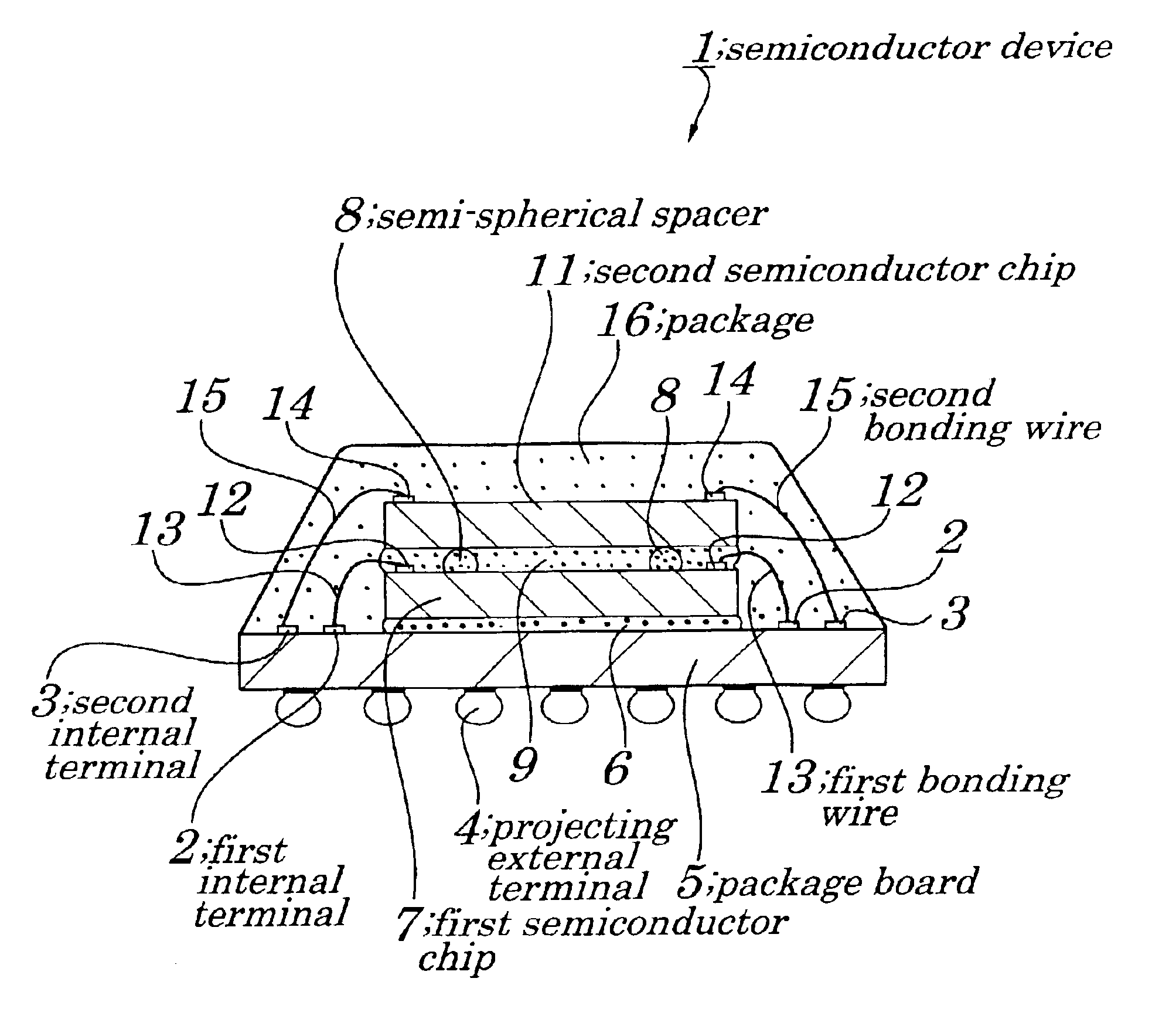
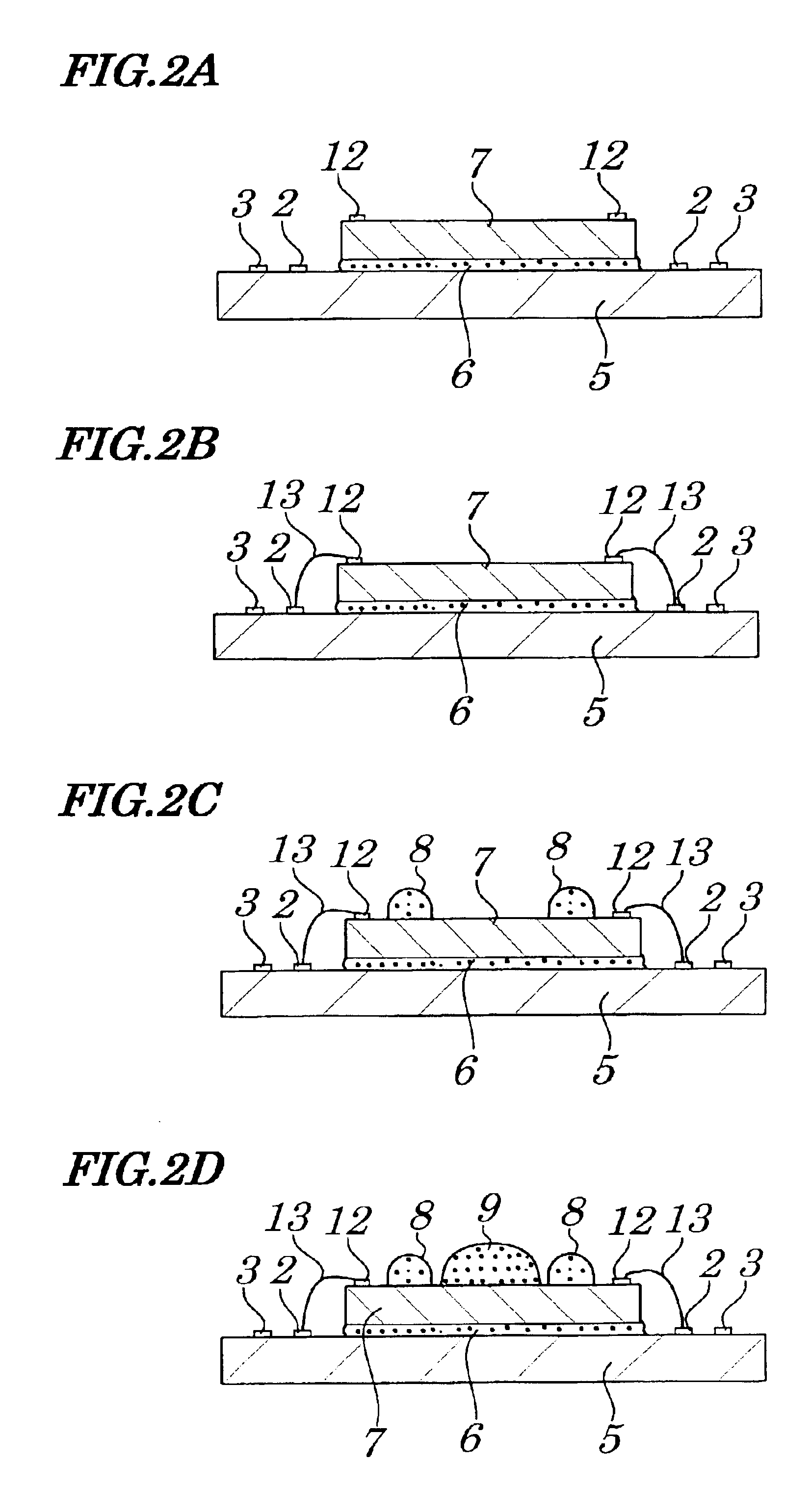
[0092]FIG. 1 is a cross-sectional view showing a configuration of a semiconductor device according to a first embodiment of the present invention; FIGS. 2A to 2G are flow diagrams for showing a first method for manufacturing the semiconductor device according to the first embodiment, along steps thereof; and FIG. 3 is an illustration for outlining one step of the first method for manufacturing the semiconductor device according to the first embodiment. As shown in FIG. 1, a semiconductor device 1 according to the present embodiment includes a first semiconductor chip (lower-layer semiconductor chip) 7 which is made of silicon and mounted (fixed) using an adhesive agent 6 on a package board 5 having a plurality of first internal terminals 2 and another plurality of second internal terminals 3 which are both formed on a right side of a surface thereof and a plurality of projecting external terminals 4 which is formed on a back side of the surface thereof; a second semiconductor chip (...

second embodiment

[0116]FIG. 7 is a cross-sectional view showing a configuration of a semiconductor device according to a second embodiment of the present invention. A semiconductor device 10 according to the present second embodiment greatly differs in configuration from that according to the above-mentioned first embodiment in a respect of stacking first and second semiconductor chips 7 and 11 one on the other via an insulating sheet 23.

[0117]That is, as shown in FIG. 7, in the semiconductor device 10 according to the present embodiment, the second semiconductor chip 11 is stacked on the first semiconductor chip 7 having roughly the same size as that thereof via a plurality of semi-spherical spacers 8 and an adhesive agent 9 as well as an insulating sheet 23. This insulating sheet 23 is made up of such a sheet as to become adhesive when heated and adhered beforehand to a back side (a surface to be adhered to the second semiconductor chip 7) of the second semiconductor chip 11.

[0118]To manufacture t...

third embodiment

[0123]FIG. 8 is a cross-sectional view showing a configuration of a semiconductor device according to a third embodiment of the present invention. A semiconductor device 20 according to the present third embodiment greatly differs in configuration from that according to the above-mentioned first embodiment in a respect of stacking a plurality of semiconductor chips in a triple stacked manner.

[0124]That is, as shown in FIG. 8, in the semiconductor device 20 according to the present embodiment, a third semiconductor chip 24 is stacked on a second semiconductor chip 11 having roughly the same size as that thereof via a plurality of semi-spherical spacers 25 and an adhesive agent 26. In this case, the semi-spherical spacers 25 and the adhesive agent 26 are made of almost the same thermo-hardening resin as the above-mentioned semi-spherical spacers 8 and the adhesive agent 9 respectively. Furthermore, a package board 27 has an addition of a plurality of third internal terminals 28 formed...


PUM


Abstract

There is provided a semiconductor device in which a plurality of semiconductor chips is stacked in layers and sealed in a package, including: a lower-layer semiconductor chip which is mounted on a package board; an upper-layer semiconductor chip which is stacked via a plurality of spacers on the lower-layer semiconductor chip; at least one first conductor interconnecting electrically at least one first electrode on the lower-layer semiconductor chip and at least one first internal terminal on the package board; at least one second conductor electrically interconnecting at least one second electrode on the upper-layer semiconductor chip and at least one second internal terminal on the package board; and the package for sealing therein the lower-layer semiconductor chip, the upper-layer semiconductor chip, and the at least one first conductor and the at least one second conductor which are all on the package board.

Description

BACKGROUND OF THE INVENTION[0001]1. Field of the Invention[0002]The present invention relates to a semiconductor device and a method for manufacturing the same and, more particularly to, the semiconductor device in which a plurality of semiconductor chips is stacked in layers on a package board and sealed in a package, and the method for manufacturing the same.[0003]The present application claims priority of Japanese Patent Application No. 2002-104570 filed on Apr. 5, 2002, which is hereby incorporated by reference.[0004]2. Description of the Related Art[0005]A Large Scale Integration (LSI), which represents semiconductor devices, has been increasingly improved in performance owing to an improvement in integration density, thus finding its applications in a variety of electronic apparatuses. Such semiconductor devices, especially those used in a mobile information processing apparatus such as a cellular phone remarkably proliferated recently, are required to be more compact in order...

Claims


Application Information

Patent Timeline
Patent Type & Authority Patents(United States)
IPC IPC(8): H01L25/065H01L25/18H01L25/07
CPCH01L24/27H01L24/29H01L24/743H01L24/83H01L25/0657H01L2924/10253H01L2224/16145H01L2224/32145H01L2224/32225H01L2224/48091H01L2224/48227H01L2224/49175H01L2224/73207H01L2224/73265H01L2224/83192H01L2224/92247H01L2225/0651H01L2225/06555H01L2225/06575H01L2924/01013H01L2924/01029H01L2924/01047H01L2924/01078H01L2924/01079H01L2924/01082H01L2924/09701H01L2924/14H01L2924/15311H01L2924/01005H01L2924/01006H01L2924/01033H01L2224/16225H01L2224/73204H01L2924/00014H01L2924/00H01L2924/00012H01L24/73H01L2924/181H01L2224/05553H01L2224/45124H01L2224/45144H01L2224/2612
Inventor KURITA, YOICHIROSHIRONOUCHI, TOSHIAKITETSUKA, TAKASHI
Owner RENESAS ELECTRONICS CORP
Why Eureka
Try Eureka