LCD device having test contact pads

a liquid crystal display and contact pad technology, applied in the direction of measurement devices, electrical testing, instruments, etc., can solve the problems of difficult manufacture of test probes, short circuit failures, and long time it takes to align the probe electrodes with respect to the contact pads, and achieve the effect of safe test operation

Inactive Publication Date: 2005-08-16
VISTA PEAK VENTURES LLC
View PDF12 Cites 54 Cited by
  • Summary
  • Abstract
  • Description
  • Claims
  • Application Information

AI Technical Summary

Benefits of technology

[0017]In accordance with the LCD device of the present invention, since the contact pads are disposed on the extension of the internal lead, the abrasion of surface or corrosion of the contact pads do not cause any malfunction in the internal lead or the elect

Problems solved by technology

However, such a test probe is difficult to manufacture, and a short-circuit failure is often caused in the conventional technique by the small pitch, involving a failure in the test operation such as a short-circuit failure.
In addition, since a high accuracy is required during the test operation in the alignment between the probe electrodes and the electrode pads (contact pads) having a small pitch and small dimensions, it takes a long time to align the probe electrodes with respect to the contact pads.
Thus, there is a problem low throughput in the test operation.
The mechanical contact between the probe electrodes and the contact pads in the LCD panel may damage the contact pads in the LCD panel by abrasion of surface or attachment of impurities thereon.
This may cause an electri

Method used


Image

  • LCD device having test contact pads
  • LCD device having test contact pads
  • LCD device having test contact pads

Examples


first embodiment

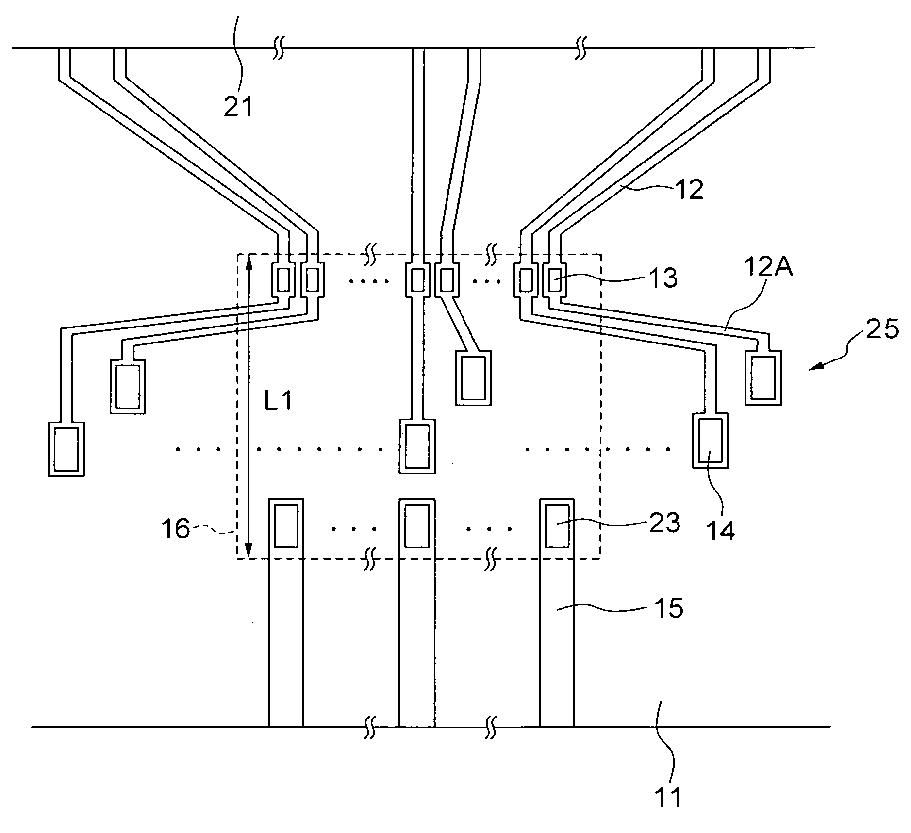
[0033]In the first embodiment, the contact pads 14 disposed apart from the electrode pads 13 and at the extensions of the internal leads 12 allow the LCD panel to be substantially free from a malfunction irrespective of occurrence of abrasion, attachment of impurities and corrosion of contact pads during the test of the LCD panel.

[0034]In addition, the pitch of extensions 12A of the internal leads 12, which is as high as around 100 μm, enables conventional probe electrodes to test the LCD panel with high reliability and high throughput irrespective of a smaller pitch which is around tens of micrometers between the electrode pads 13 for mounting the drive semiconductor chip 16.

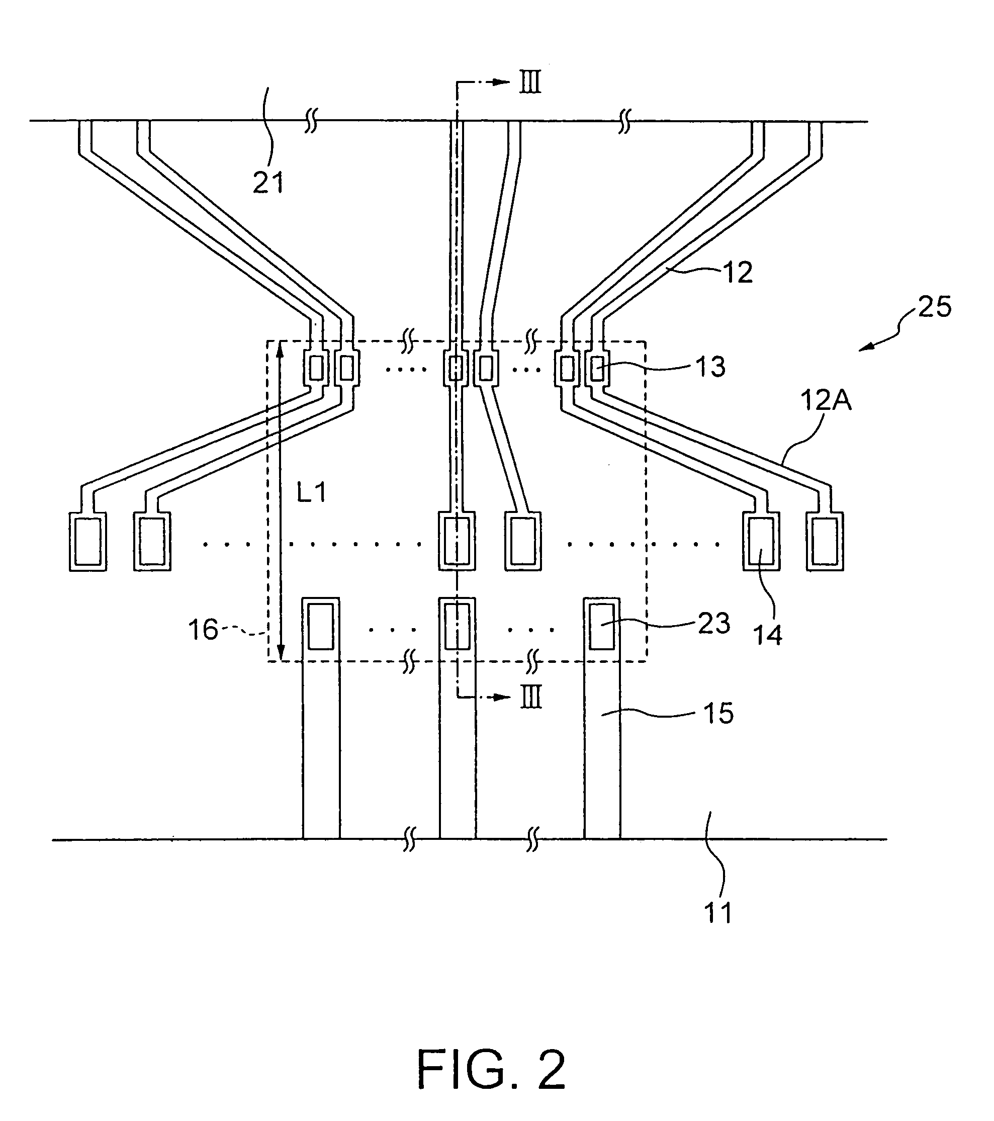
[0035]Referring to FIG. 4, a LCD device according to a second embodiment of the present invention is similar to the first embodiment except that the contact pads 14 are disposed at the extension 12A of the internal leads 12 in a staggered arrangement in the present embodiment.

[0036]It is to be noted that the pi...

third embodiment

[0044]In the third embodiment, the lengths of the extensions 12A of the internal leads 12 may be as large as several millimeters, whereby the number of steps of staggered arrangement can be increased compared to the structure shown in FIG. 4. In FIG. 5, although the two-step staggered arrangement is exemplified, the number of steps can be more than two.

[0045]For the two-step staggered arrangement shown in FIG. 5, if the pitch of the color elements is below 50 μm, 100 μm can be obtained for the pitch of the contact pads 14.

[0046]All the contact pads 14 are disposed outside the mounting area for the drive semiconductor chip 16 as shown in FIG. 5. In this case, the contact pads 14 can be used for test pads during testing the connections or signal transmissions between the drive semiconductor chip 16 and the LCD panel.

[0047]Since the above embodiments are described only for examples, the present invention is not limited to the above embodiments and various modifications or alterations c...


PUM


Abstract

To make the test probe not directly in contact with the electrode pads for the semiconductor chip mounting, without using an advanced technology for making the pitch of electrode pads narrower, and remove the chip mounting failures such as scratching of electrode pads caused by testing, adherence of impurity particles, electrical corrosion.
The electrode pads 13 formed on the distal ends of the external leads 5 for press-connecting the input electrodes 12 of the semiconductor chip 6 are disposed at both sides (shown as L1) of the semiconductor chip 6. The terminal-electrode leads 2 from the electrode pads 3 pass under the semiconductor chip 6 while keeping a pitch of the electrode pads 3. The test electrode pads 4 are disposed in alternate arrangement on the distal ends of terminal-electrode leads 2. The test electrode pads 4 may be disposed in alternate arrangement in three steps or more of multiple steps.

Description

BACKGROUND OF THE INVENTION[0001](a) Field of the Invention[0002]The present invention relates to a liquid crystal display (LCD) device having test contact pads for testing the LCD panel, and more particularly, to the structure of a LCD device for testing the LCD panel without damaging electrodes of the LCD device.[0003](b) Description of a Related Art[0004]Methods for mounting a drive semiconductor chip for driving a LCD panel in a current LCD device include a TAB (tape automated bonding) technique and a COG (chip-on-glass) technique. The TAB technique is such that the drive semiconductor chip is mounted on a TAB tape which is then connected to electrode pads formed on the LCD panel. The COG technique is such that the drive semiconductor chip is directly connected to the electrode pads of the LCD panel. The latter has advantages of smaller dimensions and lower costs compared to the former.[0005]In a LCD panel using the COG technique, since the electrode pads must be formed correspo...

Claims


Application Information

Patent Timeline
IPC IPC(8): G01R31/02G01R31/00G02F1/13G02F1/1345
CPCG02F1/13452G02F1/1309G02F1/1345
Inventor UKITA, TOORU
Owner VISTA PEAK VENTURES LLC
Why Eureka
Try Eureka