Method for manufacturing organic EL device with protective layer

a technology of organic el and protective layer, which is applied in the direction of electroluminescent light sources, transportation and packaging, coatings, etc., can solve the problems of low aggravating the quality of display, and non-luminescent areas, so as to achieve sufficient coverage, improve the moisture resistance of the protective layer, and improve the coverage of the protective layer over the surface

Inactive Publication Date: 2005-08-23
DENSO CORP
View PDF19 Cites 26 Cited by
  • Summary
  • Abstract
  • Description
  • Claims
  • Application Information

AI Technical Summary

Benefits of technology

[0008]According to the present invention, briefly, a protective layer of an organic EL device is formed by an atomic layer epitaxy (ALE) method on a surface of a luminescent structure to cover an organic luminescent material. The ALE method utilizes a reaction occurring on the surface where the protective layer is to be formed, and therefore, the protective layer can be formed uniformly along the surface. As a result, the coverage of the protective layer over the surface can be improved, and moisture resistance of the protective layer is also improved.
[0009]The protective layer may be composed of a single layer or of a plurality of layers laminated with one another. The protective layer may contain a stress relaxing component for relaxing an internal stress produced therein. When the protective layer is composed of first and second layers, the first and second layers are preferably formed to have internal stresses different from each other. Accordingly, the total stress of the protective layer can be relaxed while keeping sufficient coverage to the structure, so that the protective layer hardly has damages such as cracks due to the internal stress. The first layer and the second layer may be made of an identical material or be made of different materials from each other.

Problems solved by technology

However, it has had a problem that the organic luminescent material deteriorates due to moisture within the use environment, thus causing a non-luminescent area in the luminescent area of the structure and aggravating the quality of display.
However, according to the study conducted about the above-mentioned publication, it has been found that the moisture resistance of the protective layer is low because its coverage over the structure is insufficient and that it causes a non-luminescent area when it is operated in a high-temperature and high-moisture atmosphere (65° C. and 95% RH for example).

Method used


Image

  • Method for manufacturing organic EL device with protective layer
  • Method for manufacturing organic EL device with protective layer
  • Method for manufacturing organic EL device with protective layer

Examples


first example

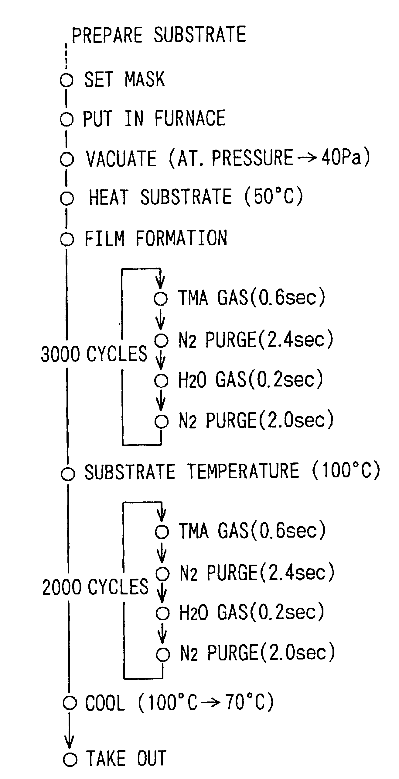
[0103]In the first example, films laminated and constituting the stress relaxing film 6 are made of the same constituent elements, and the characteristics of the films are made different from each other by changing the film formation temperatures. FIG. 10 is a flowchart showing a process for forming the protective layer 6 in this example.

[0104]First, the glass substrate 1 (35 mm×45 mm) after cleaning was put into the reaction furnace. The reaction furnace was vacuumed to about 40 Pa and the glass substrate 1 was heated while flowing N2 gas at about 400 sccm to stabilize the substrate temperature at 50° C. TMA was held within a source material bottle at 28° C. and H2O was held within another source material bottle at room temperature (24° C.). Then, TMA and H2O were gasified under the reduced pressure and were introduced to the reaction furnace with N2 gas (flow rate of 400 sccm) functioning as carrier gas.

[0105]Specifically, the gasified TMA was introduced for 0.6 seconds and then N...

second example

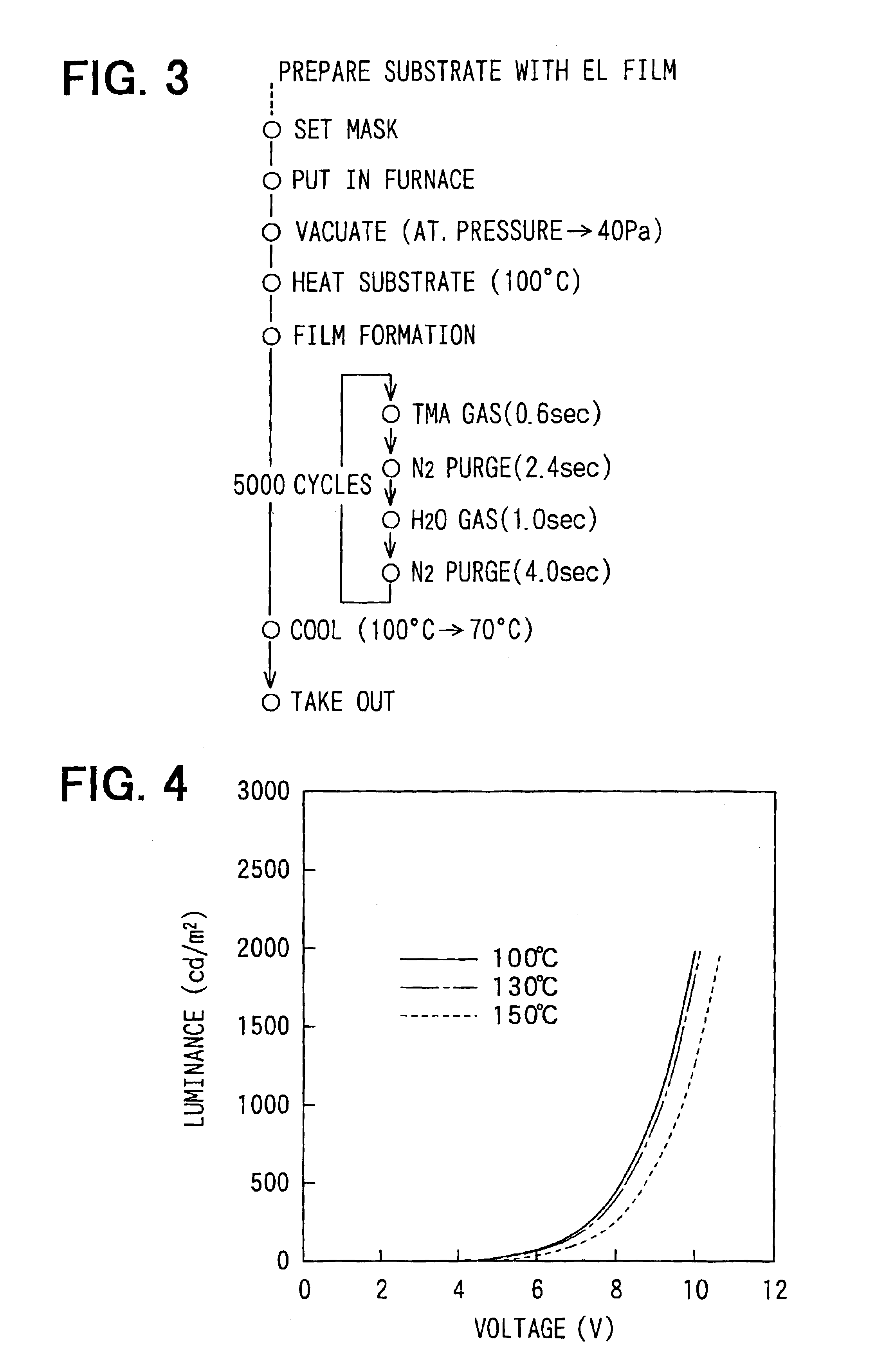
[0110]In the second example, films for constituting the protective layer 6 are formed to have different film characteristics from each other by forming them from different constituent elements from each other. FIG. 12 is a flowchart showing a process for forming the protective layer 6 in this example. Specifically, the glass substrate 1 (35 mm×45 mm) after cleaning was put into a reaction furnace. The reaction furnace was vacuumed to about 40 Pa and the glass substrate 1 was heated while flowing N2 gas at about 400 sccm to stabilize the substrate temperature at 130° C.

[0111]Then, SiCl4 and H2O were gasified within source material bottles and were introduced to the reaction furnace alternately by N2 gas (flow rate of 400 sccm) functioning as carrier gas as follows. That is, after introducing gasified SiCl4 for 1.0 second, N2 gas was introduced for 2.4 seconds. After that, gasified H2O was introduced for 3.0 seconds and N2 purge gas was introduced for 6.0 seconds in the similar manner...


PUM

PropertyMeasurementUnit
RHaaaaaaaaaa
temperatureaaaaaaaaaa
thicknessaaaaaaaaaa

Abstract

An organic EL device has a structure in which an anode, a hole transporting layer, an organic luminescent layer, and a cathode are disposed on a glass substrate in this order. The organic EL device further has a protective layer covering an outer surface of the structure to protect it from an external environment. The protective layer is formed by an ALE method at a temperature lower than glass transition temperatures materials constituting the hole transporting layer and the organic luminescent layer.

Description

CROSS REFERENCE TO RELATED APPLICATION[0001]The present application is a division of application Ser. No. 09 / 820,168, filed on Mar. 29, 2001 now abandoned, entitled ORGANIC EL DEVICE WITH PROTECTIVE LAYER, which is based upon and claims the benefit of Japanese Patent Applications No. 2000-101304 filed on Mar. 31, 2000, the contents of which are incorporated herein by reference.BACKGROUND OF THE INVENTION[0002]1. Field of the Invention[0003]This invention relates to an organic EL (electroluminescent) device comprising, on a substrate, a structure in which organic luminescent material is disposed between a pair of electrodes which face to each other, and having a protective layer for covering the organic luminescent material on the outer surface of the structure.[0004]2. Description of the Related Art[0005]In general, an organic EL device comprises, on a substrate, a structure in which organic luminescent material is disposed between a pair of electrodes that face to each other. Howev...

Claims


Application Information

Patent Timeline
Patent Type & Authority Patents(United States)
IPC IPC(8): H01L51/52H01L51/50H05B33/10H05B33/04H05B33/12H05B33/14
CPCH01L51/5237Y10T428/24942H10K59/873H10K50/8445H10K50/844
Inventor TERA, RYONOSUKEITOH, TOSHIKIYAMAMOTO, ATSUSHISUZUKI, HARUMIOZAKI, MASAAKIYAMAUCHI, TAKESHI
Owner DENSO CORP
Why Eureka
Try Eureka