Dielectric film
- Summary
- Abstract
- Description
- Claims
- Application Information
AI Technical Summary
Benefits of technology
Problems solved by technology
Method used
Image
Examples
Embodiment Construction
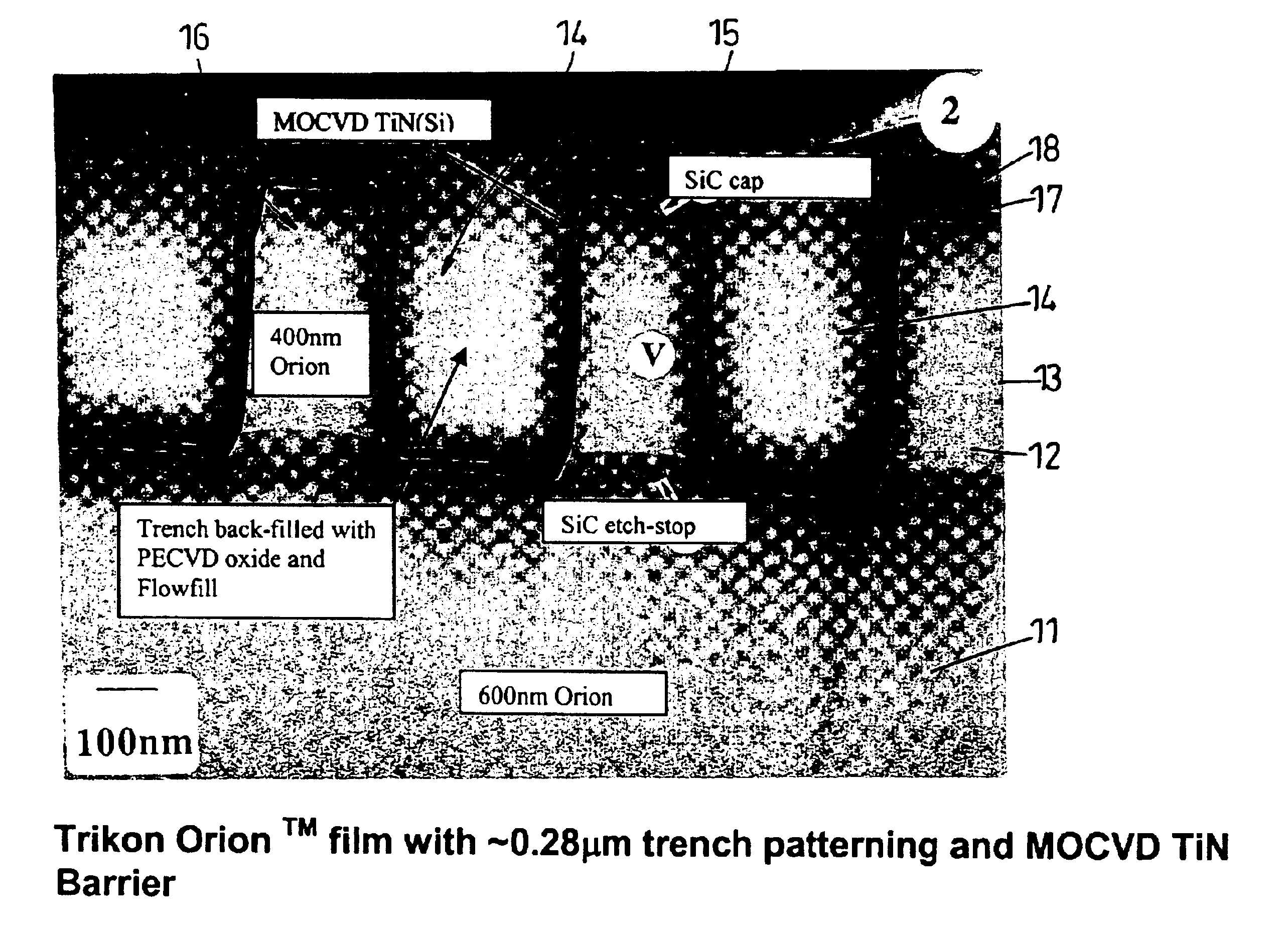
[0043]Turning to FIG. 3 a test stack is illustrated to reveal a structure common in forming damascene interconnect architecture. The stack 10 is upon a base dielectric layer 11 and consists of an etch stop layer 12, a dielectric layer 13, which has trenches 14 etched therein, a silicon carbide cap 15 on the upper surface of the dielectric layer 13 and a barrier layer 16. A silicon oxide layer 17 and a planarisation layer 18 have been added purely for the purposes of TEM sample preparation.
[0044]The dielectric layers 11 and 13 are constituted by a low k SiCOH material having more than 10% carbon, which is trade marked Orion by the Applicants. This material is porous and has a dielectric constant k of about 2.2. The planarisation layer 18 is a material which is trade marked Flowfill by the Applicants.
[0045]The dielectric layers 11 and 13 were deposited using Trikon fxP™ tool for example as described in WO-A-01 / 01472, the disclosure of which is incorporated herein by reference. This ma...
PUM
 Abstract
Description
Claims
Application Information


