Ultra wideband BGA

a technology of bga and packaging assembly, applied in the direction of semiconductor devices, semiconductor/solid-state device details, electrical apparatus, etc., can solve the problems of reducing the thermal performance of the packaging assembly, requiring costly and bulky high-frequency connectors, and limiting the performance of known bgas to certain signal speeds, etc., to achieve the effect of minimising parasitic losses

Inactive Publication Date: 2005-08-23
NORTHROP GRUMMAN SYST CORP
View PDF20 Cites 15 Cited by
  • Summary
  • Abstract
  • Description
  • Claims
  • Application Information

AI Technical Summary

Benefits of technology

[0009]In accordance with the teachings of the present invention, an electronic device packaging assembly is disclosed that includes a BGA and specialized construction to be able to operate from DC up to 50 GHz with minimal parasitic losses. The packaging assembly includes a thin base plate made of a specialized material, such as Rogers 4003, a liquid crystal polymer circuit board material, or other suitable thin organic laminates. An electronic device is mounted on the top surface of the base plate. Power vias, signal vias and ground vias are formed through the base plate and are coupled to traces, circuit components and / or the device within the packaging assembly. A cover is formed to the base plate to seal the components therein.
[0010]A specially configured impedance matching compensation network patterned on the base plate is coupled to each signal via. A ribbon bond is coupled to the compensation network and the device to provide impedance matching thereto. The compensation network includes an inductance stub and a capacitance stub to reduce parasitic inductive and capacitive losses. A ball is mounted to a back surface of the base plate to provide high speed electrical connections to the vias. Solder balls in the BGA have a certain size and pitch suitable for high frequency applications. The solder balls used for signal connections are separated from other solder balls in the array to form a coaxial structure.

Problems solved by technology

Existing electronic packaging assemblies sometimes include high speed input / output (I / O) ports that require costly and bulky high frequency connectors to provide the high speed.
However, as the ceramic thickness increases, the thermal performance of the packaging assembly decreases.
Known BGAs are realistically limited in their performance to under certain signal speeds.
Parasitic capacitances and inductances from the device packaging severely affect device performance for the known packaging assemblies above these signal speeds.
However, LGAs and LCCs have the drawback of thermal cycling problems.
Further, LCCs cannot be utilized for more than a certain size, which is dependant on differences between the package and circuit board material's coefficient of thermal expansion (CTE).
For higher frequencies, the electrical leads that are formed to accommodate environmental extremes typically cause increased inductance and signal radiation, which is difficult to accommodate for.

Method used


Image

  • Ultra wideband BGA
  • Ultra wideband BGA
  • Ultra wideband BGA

Examples


Embodiment Construction

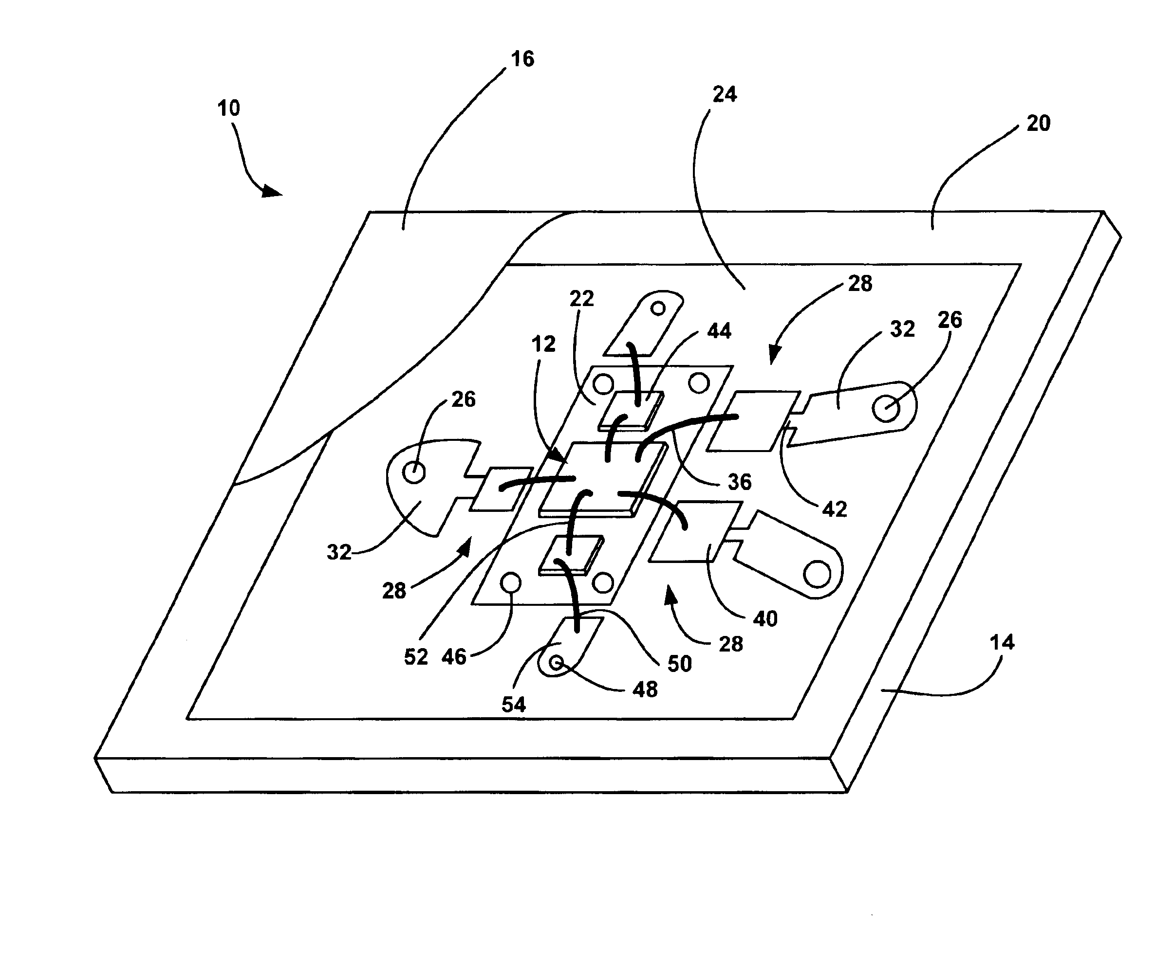
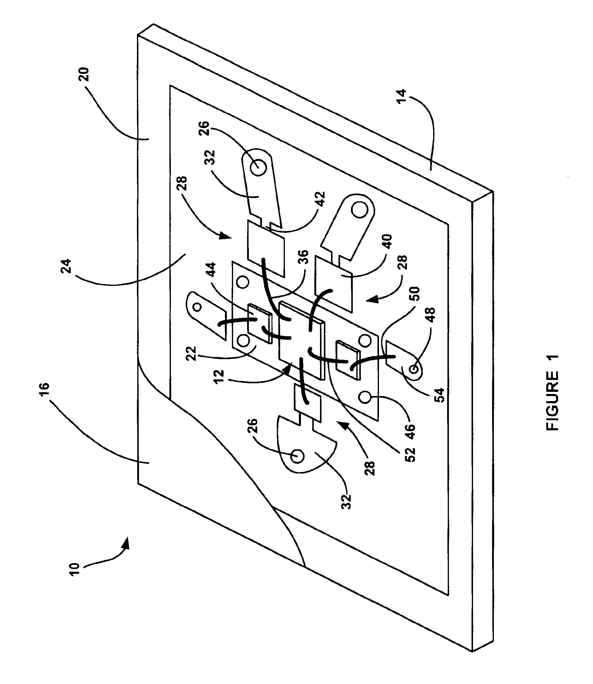
[0014]The following description of the embodiments of the invention directed to a high speed device packaging assembly for an electronic device including a ball grid array is merely exemplary in nature, and is in no way intended to limit the invention or its applications or uses.

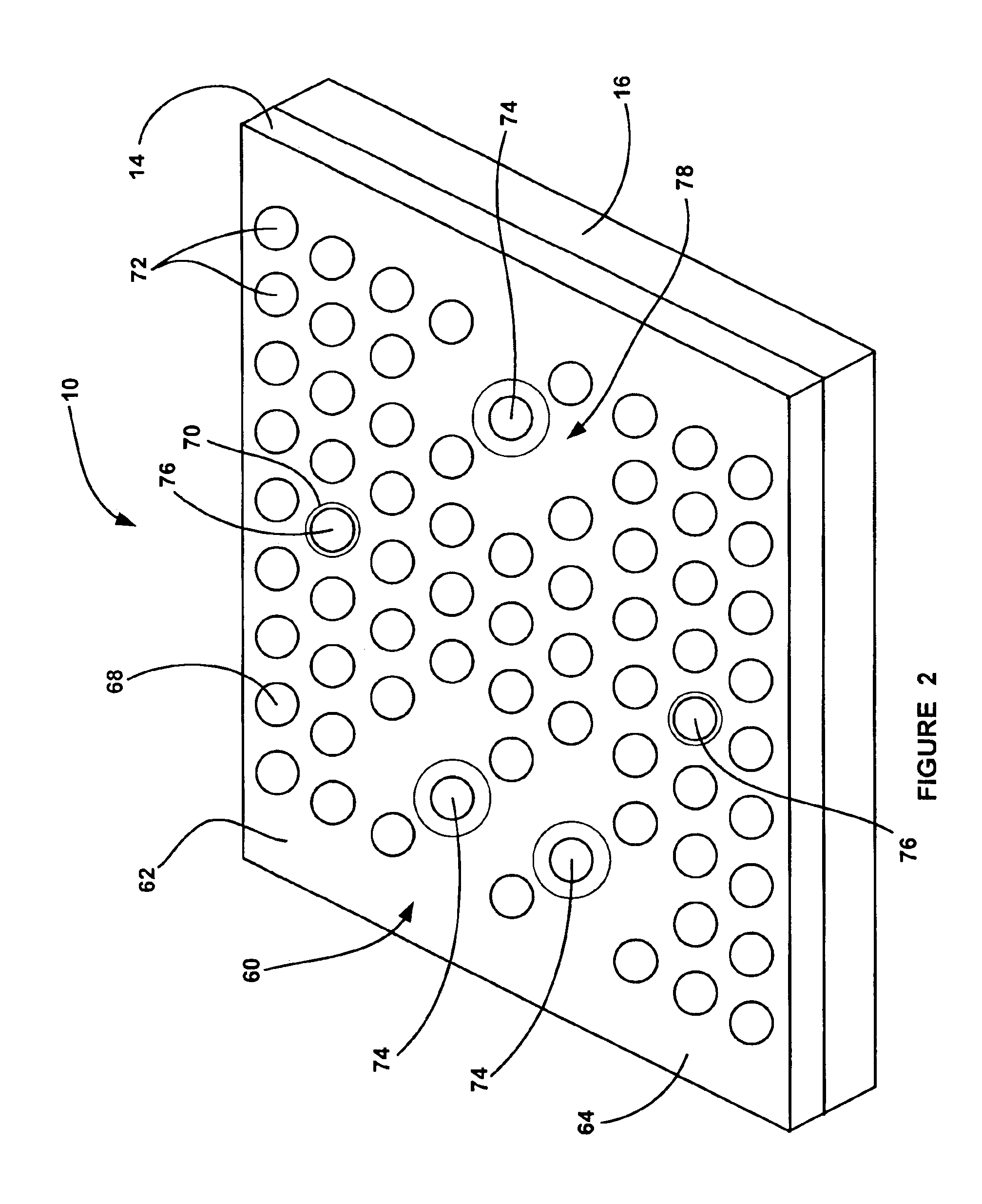
[0015]FIG. 1 is a perspective view of a package assembly 10 for enclosing a high speed electronic device 12, such as an amplifier, filter, RAM, etc. The assembly 10 includes a base plate 14 to which the device 12 is mounted, as shown. The base plate 14 is made of a special laminate material, for example, a fiber and resin mixture, such as Rogers 4003, a liquid crystal polymer (LCP) circuit board material or other suitable thin organic laminates, that provide a rigid support. By using these types of materials, the base plate 14 can be made very thin, thus reducing the length of the vias and interconnections, discussed below, that would otherwise have significant drawbacks from parasitic inductances and capaci...


PUM


Abstract

An electronic device packaging assembly (10) that includes a ball grid array (60) and specialized construction to be able to operate from DC up to 50 GHz with minimal parasitic losses. The packaging assembly (10) includes a thin base plate (14) made of a suitable rigid material. Power vias (48), signal vias (26) and ground vias (46) are formed through the base plate (14) to be coupled to traces, circuit components, and / or the device (12) within the packaging assembly (10). An impedance matching compensation network (28) provides impedance matching between the device (12) and the signal vias (26). The ball grid array (60) includes a plurality of solder balls (68), including ground solder balls (72), signal solder balls (74) and power solder balls (76), electrically coupled to the appropriate via extending through the base plate (14).

Description

BACKGROUND OF THE INVENTION[0001]1. Field of the Invention[0002]This invention relates generally to an electronic device ball grid array (BGA) packaging assembly and, more particularly, to an electronic device BGA packaging assembly, including a thin laminate base plate, that is designed to operate from DC up to 50 GHz with minimal parasitic losses.[0003]2. Discussion of the Related Art[0004]Chip scale packaging is a known technique for environmentally protecting and configuring an electronic chip device and associated circuits within a packaging assembly. Specialized lead frames and circuit connectors are required to electrically couple the electronic device and associated circuits to the various signal lines, power lines and ground lines through the package. Existing electronic packaging assemblies sometimes include high speed input / output (I / O) ports that require costly and bulky high frequency connectors to provide the high speed.[0005]A ball grid array (BGA) is one known I / O de...

Claims


Application Information

Patent Timeline
Patent Type & Authority Patents(United States)
IPC IPC(8): H01L23/498H01L23/48H01L23/12H01L23/50H01L23/66
CPCH01L23/50H01L23/66H01L24/49H01L23/49816H01L2224/45014H01L2224/48091H01L2224/49171H01L2924/01002H01L2924/01004H01L2924/01006H01L2924/01013H01L2924/01028H01L2924/01029H01L2924/01033H01L2924/01047H01L2924/01079H01L2924/01082H01L2924/19041H01L2924/19105H01L2924/30105H01L2924/30107H01L2924/3011H01L2924/00014H01L24/45H01L24/48H01L2924/014H01L2224/48227H01L2924/00H01L2924/30111H01L2224/48195H01L2224/45099H01L2924/206
Inventor HATHAWAY, JAMES A.CROSSMAN, BRIAN F.DIN, SALAH
Owner NORTHROP GRUMMAN SYST CORP
Why Eureka
Try Eureka