Non-contact mobile charge measurement with leakage band-bending and dipole correction

a mobile charge and measurement method technology, applied in the field of non-contact mobile charge measurement with leakage band bending and dipole correction, can solve the problems of static charging of the insulator surface, poor oxide/silicon interface formation, and excessive ionic contamination of the insulator bulk

Inactive Publication Date: 2005-08-30
FUNG MIN SU +3
View PDF9 Cites 10 Cited by
  • Summary
  • Abstract
  • Description
  • Claims
  • Application Information

AI Technical Summary

Problems solved by technology

These induced charges can result from static charging of insulator surfaces, poorly formed oxide / silicon interfaces and excessive ionic contamination within the insulator bulk.
Some sources of sodium can be contaminated quartz ware, incompletely removed photoresist and inadvertent human contact.
Although widely accepted, the MOS methods have increasingly unacceptable high cost and excessive time associated with the MOS sample preparation.
For monitoring thick oxides, the sample preparation time for aluminum MOS electrodes can be 1-2 days and for thin oxides, the cost and time for fabricating polysilicon electrodes is even worse.
Furthermore, the fabrication process for these MOS electrodes can become a source for sodium or other measurement complications.

Method used


Image

  • Non-contact mobile charge measurement with leakage band-bending and dipole correction
  • Non-contact mobile charge measurement with leakage band-bending and dipole correction

Examples


Embodiment Construction

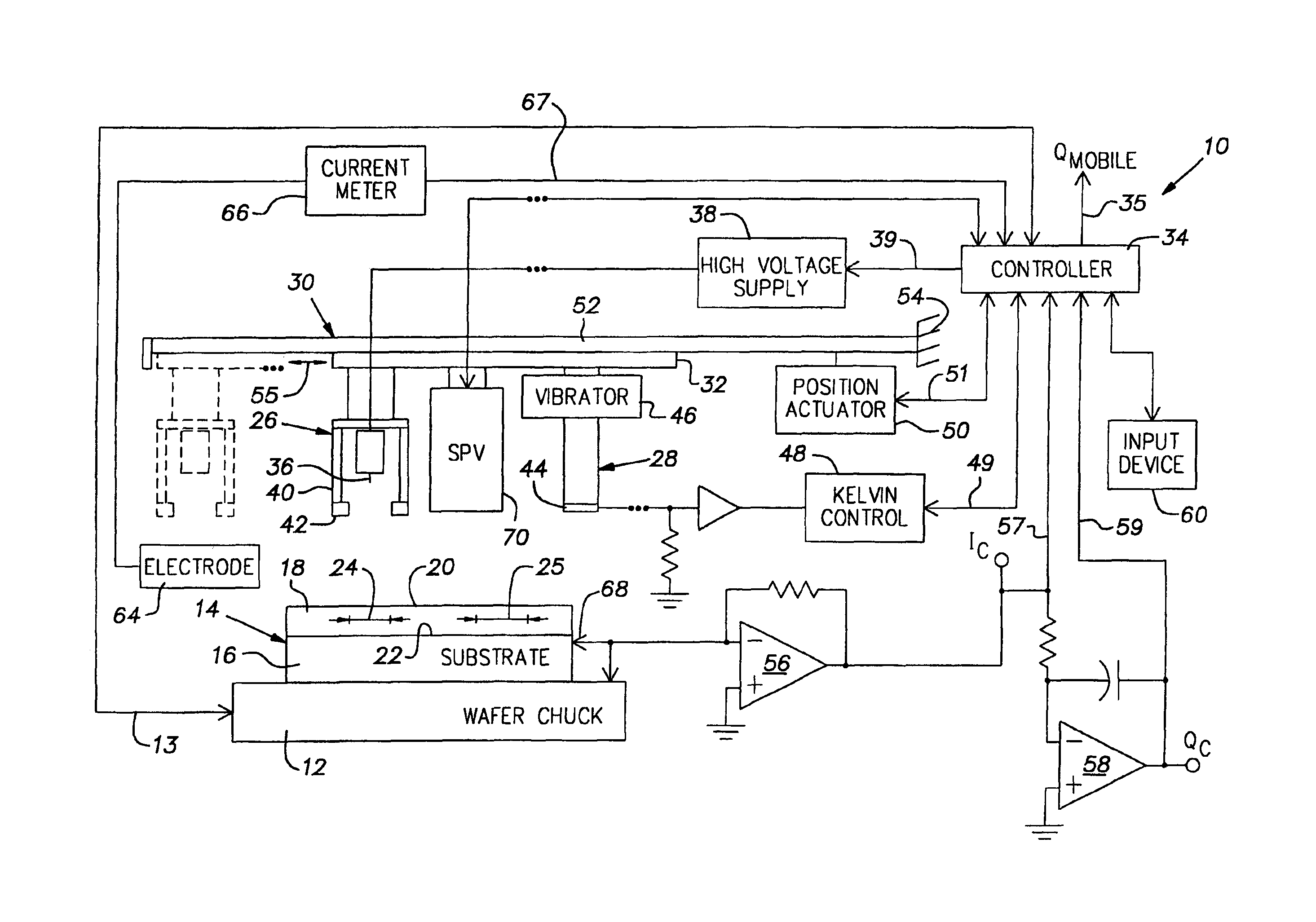
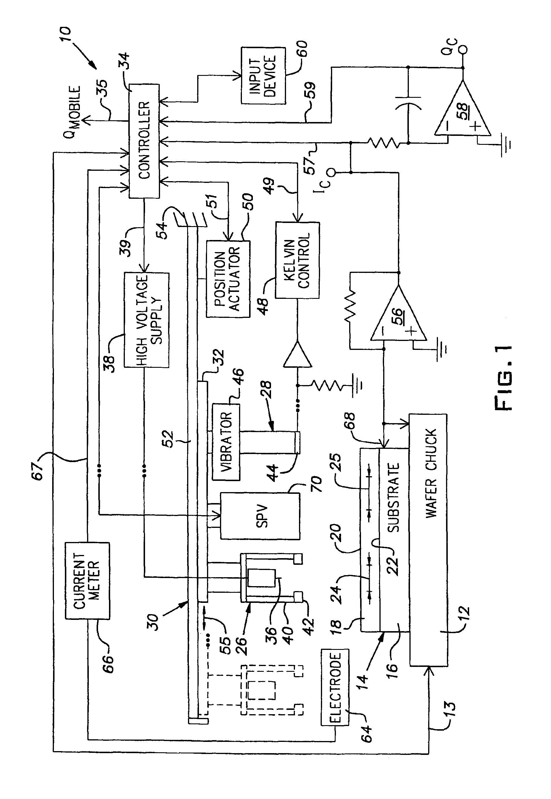
[0012]Referring to FIG. 1, a contactless corona-oxide-semiconductor mobile ionic charge measurement apparatus, generally referred to by numeral 10, is shown. The apparatus 10 includes, in part, a temperature controllable wafer chuck 12, for heating and cooling a semiconductor wafer 14 to be tested. The wafer 14 includes a semiconductor substrate 16 (e.g., doped silicon) having a dielectric layer 18 (e.g., silicon dioxide) thereon. The surface of the wafer 14 also has an air / dielectric boundary surface 20 and a dielectric / substrate boundary surface 22. A measurement region 24 and a measurement region 25 depict respective regions of the dielectric layer 18 selected for testing.

[0013]A calibrated corona discharge source or corona gun 26 is provided for depositing corona charge on the surface 20 of the dielectric layer 18. An electrostatic measurement device or Kelvin probe 28 enables a surface voltage potential of the wafer 14 to be measured. A surface photovoltage measurement (SPV) to...


PUM


Abstract

Corona charges are used to bias a wafer to push down mobile charges and then pull them up during temperature cycles. Mobile charge is measured from the drops in the corona voltage due to the mobile charges. Corrections are made in the measurements for dipole potentials, leakage and silicon band-bending.

Description

[0001]This application is a divisional application of U.S. patent application Ser. No. 10 / 298,778, filed Nov. 18, 2002, now U.S. Pat. No. 6,771,092 which was a divisional application of U.S. patent application Ser. No. 08 / 847,644, filed Apr. 30, 1997, which issued as U.S. Pat. No. 6,522,158 on Feb. 18, 2003.BACKGROUND OF THE INVENTION[0002]The present invention relates to the field of semiconductor wafer testing and, more particularly, to a non-contact method for testing such wafers.[0003]In the semiconductor industry, the behavior of FET and bipolar devices used to fabricate integrated circuits are very sensitive to induced charges on the silicon wafers. These induced charges can result from static charging of insulator surfaces, poorly formed oxide / silicon interfaces and excessive ionic contamination within the insulator bulk.[0004]The most prevalent source of ionic contamination is sodium. Other less prevalent sources are potassium and lithium. Some sources of sodium can be conta...

Claims


Application Information

Patent Timeline
Patent Type & Authority Patents(United States)
IPC IPC(8): G01R31/311G01R31/28
CPCG01R31/311
Inventor FUNG, MIN-SUVERKUIL, ROGER L.HORNER, GREGORY S.HOWLAND, WILLIAM H.
Owner FUNG MIN SU
Why Eureka
Try Eureka