Address conversion unit for memory device

a technology of address conversion unit and memory device, which is applied in memory adressing/allocation/relocation, program control, instruments, etc., can solve the problems of large table size, slower speed of writing data into flash memory, etc., and achieve the effect of reducing the volume of valid logical blocks and high speed

Inactive Publication Date: 2005-08-30
PANASONIC CORP
View PDF11 Cites 30 Cited by
  • Summary
  • Abstract
  • Description
  • Claims
  • Application Information

AI Technical Summary

Benefits of technology

[0015]The present invention is proposed to settle the above-mentioned problems, and has an object to provide a address conversion unit for a memory device that can control the mass of the storage medium by a compact control circuit, and access written data at high speed.
[0018]The logical address is converted to the physical address by using the above two tables, so that the capacity of the first table can be reduced.
[0019]Moreover, in order to promote efficiency to form the logical blocks containing data blocks, and read or erase the logical block, the present invention is provided with a physical block table, a logical block table, an entry counter, and an address register.
[0024]As described above, upon receipt of a request to read the logical block specified by the specific logical address, the reading means reads the information stored in the second table by means of the logical address, and then obtains the physical address of the representative page. According to the obtained physical address of the representative page, the reading means reads chain information which was written into the representative page. The chain information is the physical address of the other page contained in the same logical block as the representative page. After reading the chain information, the reading means obtains the physical address of the other page. According to the obtained physical address of the other page, the reading means reads the chain information written into the other page and then obtains the physical address of the different other page. In this way, the reading means can obtains the physical addresses of all the pages contained in the logical block corresponding to the read request.
[0027]The erasing means erases the data stored in the selected physical blocks as follows. The erasing means refers to the physical block table, the logical block table, and the address register, and then determines the physical blocks on which a small number of the valid logical blocks are formed. The erasing means determines the physical blocks to be erased, and copies the valid logical blocks formed on the erase-target physical blocks to the other physical blocks. And then the erase-target physical blocks are erased. By determining the erase-target physical blocks in this way it is possible to decrease the volume of the valid logical blocks to be copied at erasing the data. Therefore, the data erasing can be processed at high speed.

Problems solved by technology

However, the speed of writing data into the flash memory is slower than the speed of transferring data to a buffer in the memory device, whereby a wait time is generated.
However, the more the storage capacity increases, the larger the table becomes in size.
Furthermore, the effective writing method for the flash memory has been disclosed in the aforementioned prior art, while no prior art discloses a method for writing data which a reading means can access at high-speed.

Method used


Image

  • Address conversion unit for memory device
  • Address conversion unit for memory device
  • Address conversion unit for memory device

Examples


first embodiment

(First Embodiment)

[Operations at the Time of Power-On]

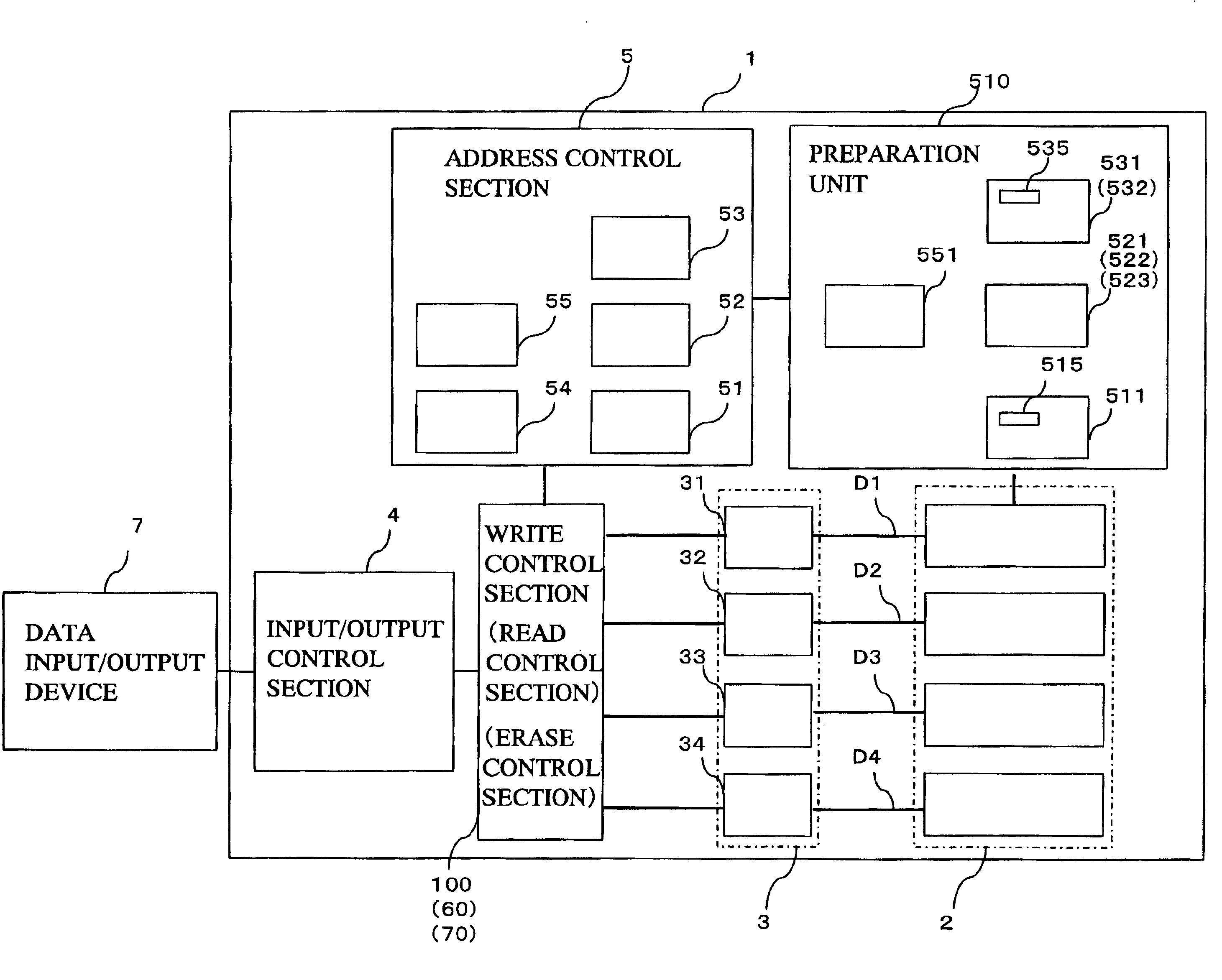
[0047]When power is turned on in the memory device 1, a physical block table preparation means 521 provided to a preparation means 510 prepares a physical block table 52. And the physical block table 52 is prepared on RAM of an address control means 5 provided to the memory device 1. FIG. 3 shows an example of steps for preparing the physical block table 52.

[0048]First of all, the physical block table preparation means 521 initializes all values in the physical block table 52 (S301 in FIG. 3). By the initialization in this embodiment, all the values of the physical block table 52 are changed to ‘blank’ so as to represent that each physical block has no data.

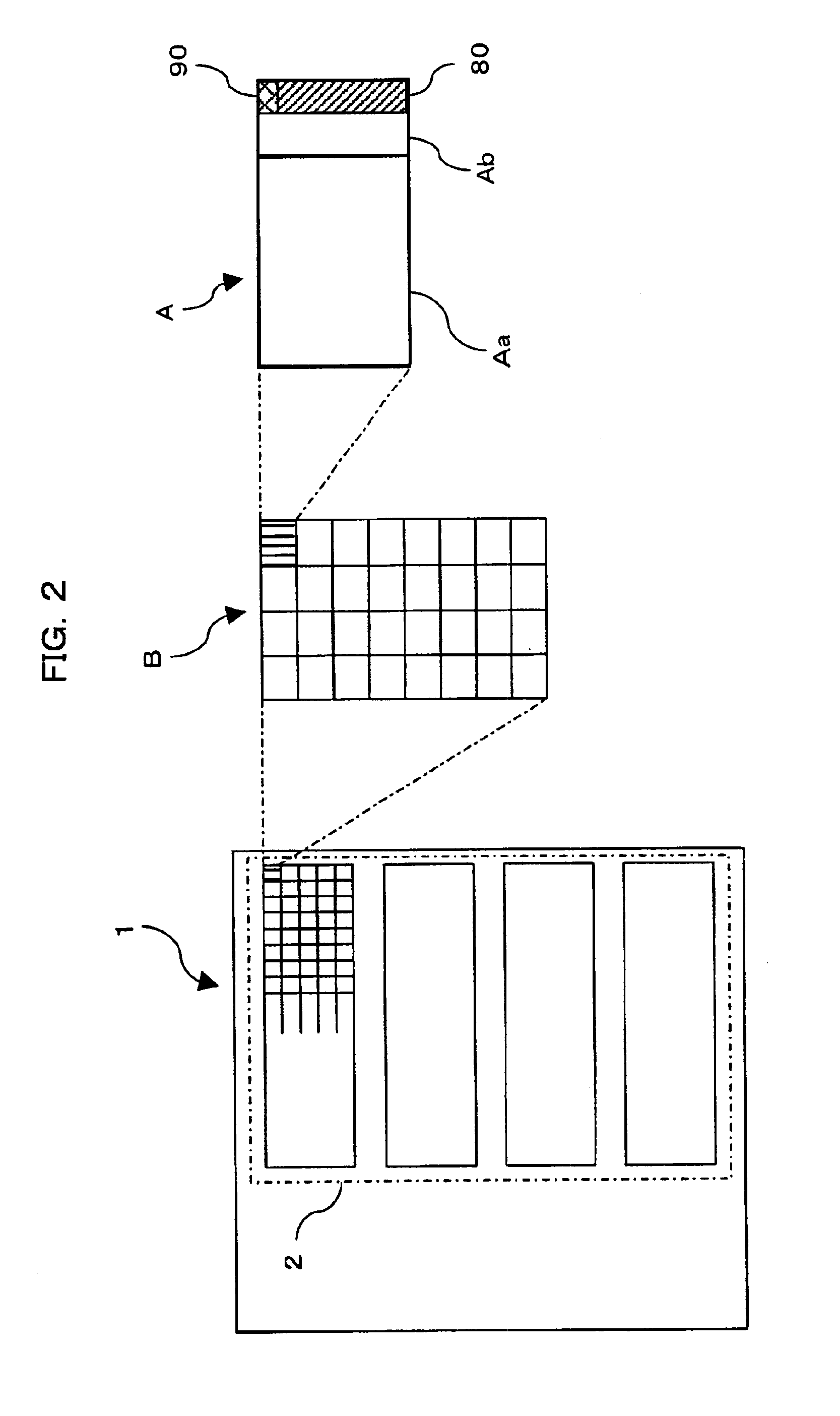
[0049]Subsequently, the physical block table preparation means 521 actually confirm a state of a specific physical block B (S302 in FIG. 3). The state of the specific physical block B can be known by confirming a specific page A contained in the specific physical block B shown...

second embodiment

(Second Embodiment)

[0163]In the above description, the writing means 100 determines the second table 80 as the invalid table, and the value of the flag section 90 in Page A storing the invalid second table 80 is updated to an invalid value by the writing means 100. In order to perform the writing as fast as possible, however, such updating operation should be eliminated.

[0164]The achieve the above object, the writing means 100 determines Page A into which the rewrite table read onto the buffers 31 to 34 is written, in a manner as described below, and then copies the second table 80 to the determined Page A.

[0165]First of all, regarding pages A within the same physical block B that the invalid table is stored, the writing means 100 determines whether or not there are available pages A having the physical address that is larger than the page A storing the invalid table, and includes the specific 5 bits—‘01000’. In this embodiment, the second table 80 can be stored only in Page A of wh...


PUM


Abstract

A memory device with a nonvolatile memory and RAM for accessing the nonvolatile memory is generally provided with a table to convert a logical address to a physical address, however, in the invention, the table is divided to a first table on RAM and a second table on the nonvolatile memory. The first table converts specific bits of the logical address to a first physical address indicating a location of the second table. The second table converts the other bits of the logical address to a physical address of a representative page of pages contained in a storage area corresponding to the logical address. A unit operable to access data (a writing unit operable to, a reading unit operable to, and an erasing unit operable to) reaches a target physical address based on the logical address. Such configuration can reduce the capacity of each conversion table.

Description

BACKGROUND OF THE INVENTION[0001]1. Field of the Invention[0002]The present invention relates to an address conversion unit for a memory device provided with a nonvolatile memory such as a flash memory capable of rewriting data therein.[0003]2. Description of Related Art[0004]The portable device for music data and video data has begun using a memory device provided with a nonvolatile memory such as a flash memory. The flash memory allows data to be rewritten, has a high portability, and requires no back-up power such as a battery or the like.[0005]However, the speed of writing data into the flash memory is slower than the speed of transferring data to a buffer in the memory device, whereby a wait time is generated.[0006]A conventional method of efficiently writing data into the flash memory is disclosed in Japanese Laid open Publication No. 06-301601, in which the data is written in parallel into a plurality of physical blocks.[0007]In addition, in order to access a data stored in t...

Claims


Application Information

Patent Timeline
Patent Type & Authority Patents(United States)
IPC IPC(8): G06F12/02G06F12/00G06F12/16
CPCG06F12/0246G06F12/0292G06F2212/2022G06F2212/7201G06F12/00
Inventor TOYAMA, MASAYUKISEKIBE, TSUTOMU
Owner PANASONIC CORP
Why Eureka
Try Eureka