Formation of composite tungsten films

a composite tungsten and film technology, applied in the direction of crystal growth process, polycrystalline material growth, chemically reactive gas growth process, etc., can solve the problems of difficult sub-micron structure filling and unreliable integrated circuit performan

Inactive Publication Date: 2005-09-06
APPLIED MATERIALS INC
View PDF76 Cites 104 Cited by
  • Summary
  • Abstract
  • Description
  • Claims
  • Application Information

AI Technical Summary

Benefits of technology

[0009]A method of depositing a composite tungsten (W) film on a substrate is provided. The composite tungsten (W) film comprises a tungsten (W) bulk layer formed on a tungsten (W) nucleation layer. The tungsten nucleation layer may be formed using a cyclical deposition process by alternately adsorbing a tungsten-containing precursor and a reducing gas on the substrate. The tungsten-containing precursor and the reducing gas react to form the tungsten layer on the substrate. The tungsten bulk layer may be formed using a chemical vapor deposition (CVD) process by thermally decomposing a tungsten-containing precursor.
[0010]Thus, the present invention provides a method of forming a composite tungsten layer comprising inserting a substrate into a process chamber and introducing a tungsten precursor to the process chamber. The tungsten precursor is allowed to adsorb onto the substrate. Next, a reducing gas is introduced into the process environment and is allowed to adsorb onto the substrate, and, at this point, a tungsten nucleation film is formed on the substrate. The steps of introducing and adsorbing the precursor and reducing gas are repeated until a desired thickness of the tungsten nucleation film layer is formed. Once a desired thickness of nucleation film is achieved, a tungsten bulk layer is then formed on the nucleation layer.

Problems solved by technology

Many traditional deposition processes (e.g., chemical vapor deposition (CVD) and physical vapor deposition (PVD)) have difficulty filling sub-micron structures where the aspect ratio exceeds 6:1, and especially where the aspect ratio exceeds 10:1.
The presence of either voids or seams may result in unreliable integrated circuit performance.

Method used


Image

  • Formation of composite tungsten films
  • Formation of composite tungsten films
  • Formation of composite tungsten films

Examples


Embodiment Construction

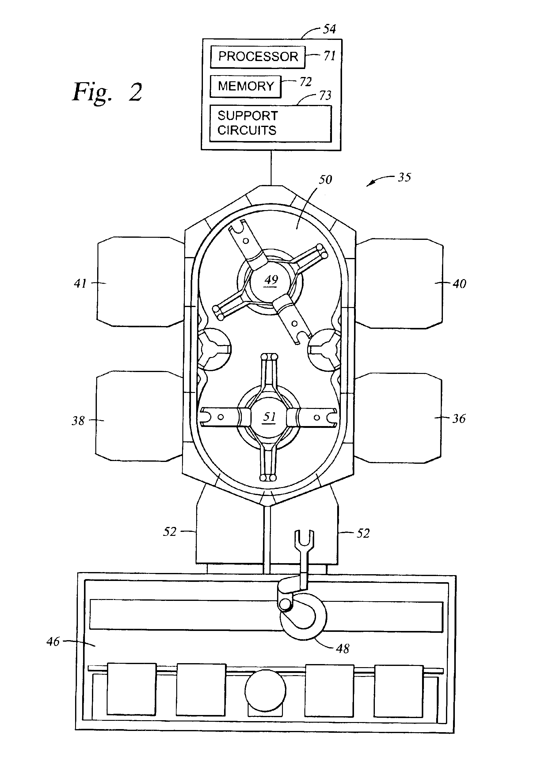
[0024]FIG. 2 is a schematic representation of a wafer processing system 35 that can be used to perform tungsten deposition in accordance with embodiments described herein. The wafer processing system 35 typically comprises process chambers 36, 38, 40, 41, transfer chamber 50, load-lock chambers 52, a factory interface 46, a microprocessor controller 54, along with other hardware components such as power supplies (not shown) and vacuum pumps (not shown). An example of such a wafer processing system 35 is an ENDURA SL system, available from Applied Materials, Inc., Santa Clara, Calif.

[0025]Details of the wafer processing system 35 are described in commonly assigned U.S. patent application Ser. No. 09 / 451,628, entitled “Integrated Modular Processing Platform”, filed on Nov. 30, 1999, which is hereby incorporated herein by reference. The salient features of the wafer processing system 35 are briefly described below.

[0026]The wafer processing system 35 includes a transfer chamber 50 cont...


PUM

PropertyMeasurementUnit
temperatureaaaaaaaaaa
pressureaaaaaaaaaa
temperatureaaaaaaaaaa

Abstract

Methods for the deposition of tungsten films are provided. The methods include depositing a nucleation layer by alternatively adsorbing a tungsten precursor and a reducing gas on a substrate, and depositing a bulk layer of tungsten over the nucleation layer.

Description

CROSS-REFERENCE TO RELATED APPLICATIONS[0001]This application is a continuation of PCT patent application serial number PCT / US02 / 22585, filed Jul. 16, 2002, which claims benefit of U.S. provisional patent application Ser. No. 60 / 306,027, filed Jul. 16, 2001.BACKGROUND OF THE INVENTION[0002]1. Field of the Invention[0003]Embodiments of the present invention relate generally to a method of tungsten film formation.[0004]2. Description of the Related Art[0005]Reliably producing sub-half micron and smaller features is one of the key technologies for the next generation of very large scale integrated (VLSI) circuits as well as ultra large scale integrated (ULSI) circuits. In particular, as the fringes of integrated circuit technology are pressed, the shrinking dimensions of interconnect features in VLSI and ULSI technology have placed additional demands on processing capabilities to increase both circuit density and the quality of integrated circuits. For example, multi-level interconnect...

Claims


Application Information

Patent Timeline
Patent Type & Authority Patents(United States)
IPC IPC(8): C23C16/06C23C16/14C23C16/02H01L21/285H01L21/70H01L21/02H01L21/768C23C16/44C23C16/04C23C16/08C23C16/455H01L21/28
CPCC23C16/0281C23C16/08C23C16/14C23C16/45523C23C16/45525H01L21/28556H01L21/28562H01L21/76843H01L21/76876H01L21/76877
Inventor LAI, KEN K.BYUN, JEONG SOOWU, FREDERICK C.SRINIVAS, RAMANUJAPURAN A.GELATOS, AVGERINOSCHANG, MEIKORI, MORISSINHA, ASHOK K.CHUNG, HUAFANG, HONGBINMAK, ALFRED W.YANG, MICHAEL X.XI, MING
Owner APPLIED MATERIALS INC
Why Eureka
Try Eureka