Pulsed nucleation deposition of tungsten layers

a technology of tungsten and tungsten layers, applied in the direction of polycrystalline material growth, crystal growth process, chemically reactive gas, etc., can solve the problems of increasing stringent requirements for step coverage and layer uniformity, tungsten layers, for example, are particularly difficult to deposit, etc., and achieve good step coverage

Inactive Publication Date: 2007-05-01
APPLIED MATERIALS INC
View PDF408 Cites 143 Cited by
  • Summary
  • Abstract
  • Description
  • Claims
  • Application Information

AI Technical Summary

Benefits of technology

[0008]Embodiments of the present invention generally relate to a method of forming a tungsten nucleation layer using a sequential deposition process. The tungsten nucleation layer is formed by reacting pulses of a tungsten-containing precursor and a reducing gas in a process chamber to deposit tungsten on the substrate. Thereafter, reaction by-products generated from the tungsten deposition are removed from the process chamber. After the reaction by-products are removed from the process chamber, a flow of the reducing gas is provided to the process chamber to react with residual tungsten-containing precursor remaining therein. Such a deposition process forms tungsten nucleation layers having good step coverage. The sequential deposition process of reacting pulses of the tungsten-containing precursor and the reducing gas, removing reaction by-products, and than providing a flow of the reducing gas to the process chamber may be repeated until a desired thickness for the tungsten nucleation layer is formed.

Problems solved by technology

Integrated circuits have evolved into complex devices that can include millions of components (e.g., transistors, capacitors and resistors) on a single chip.
In particular, metal layers, such as those used for interconnect, contact, and plug fill applications, are subject to increasingly stringent requirements related to step coverage and layer uniformity.
Tungsten layers, for example, are particularly difficult to deposit with uniform step coverage.
As a result, voids may form in the tungsten nucleation layer during deposition, adversely impacting the electrical performance of devices fabricated therefrom.

Method used


Image

  • Pulsed nucleation deposition of tungsten layers
  • Pulsed nucleation deposition of tungsten layers
  • Pulsed nucleation deposition of tungsten layers

Examples


Embodiment Construction

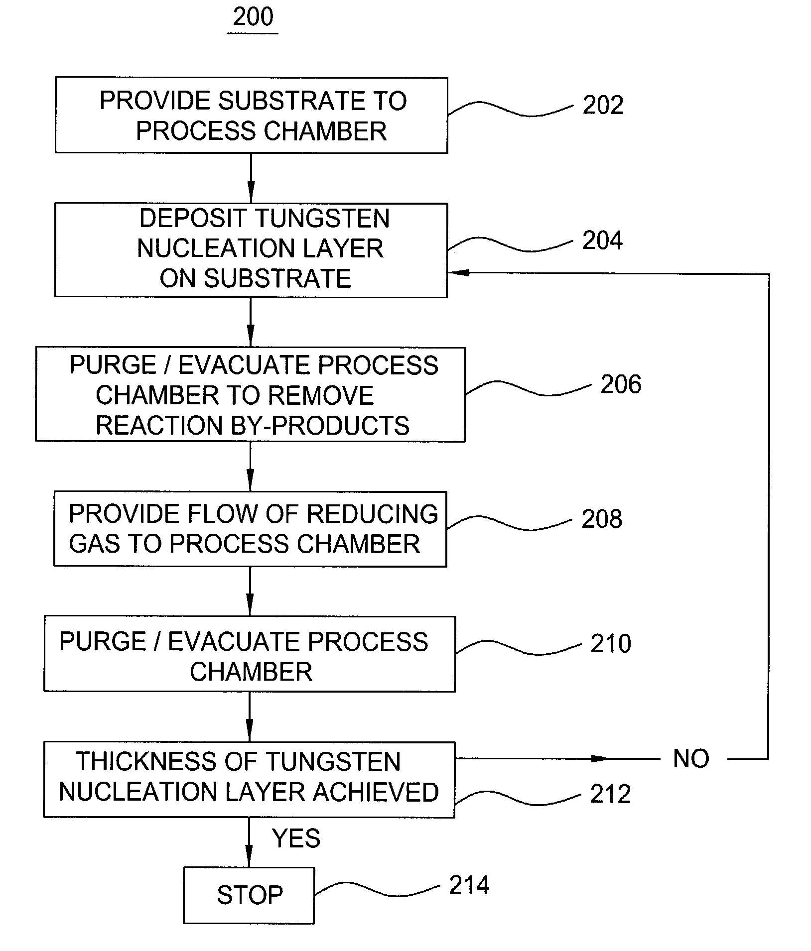
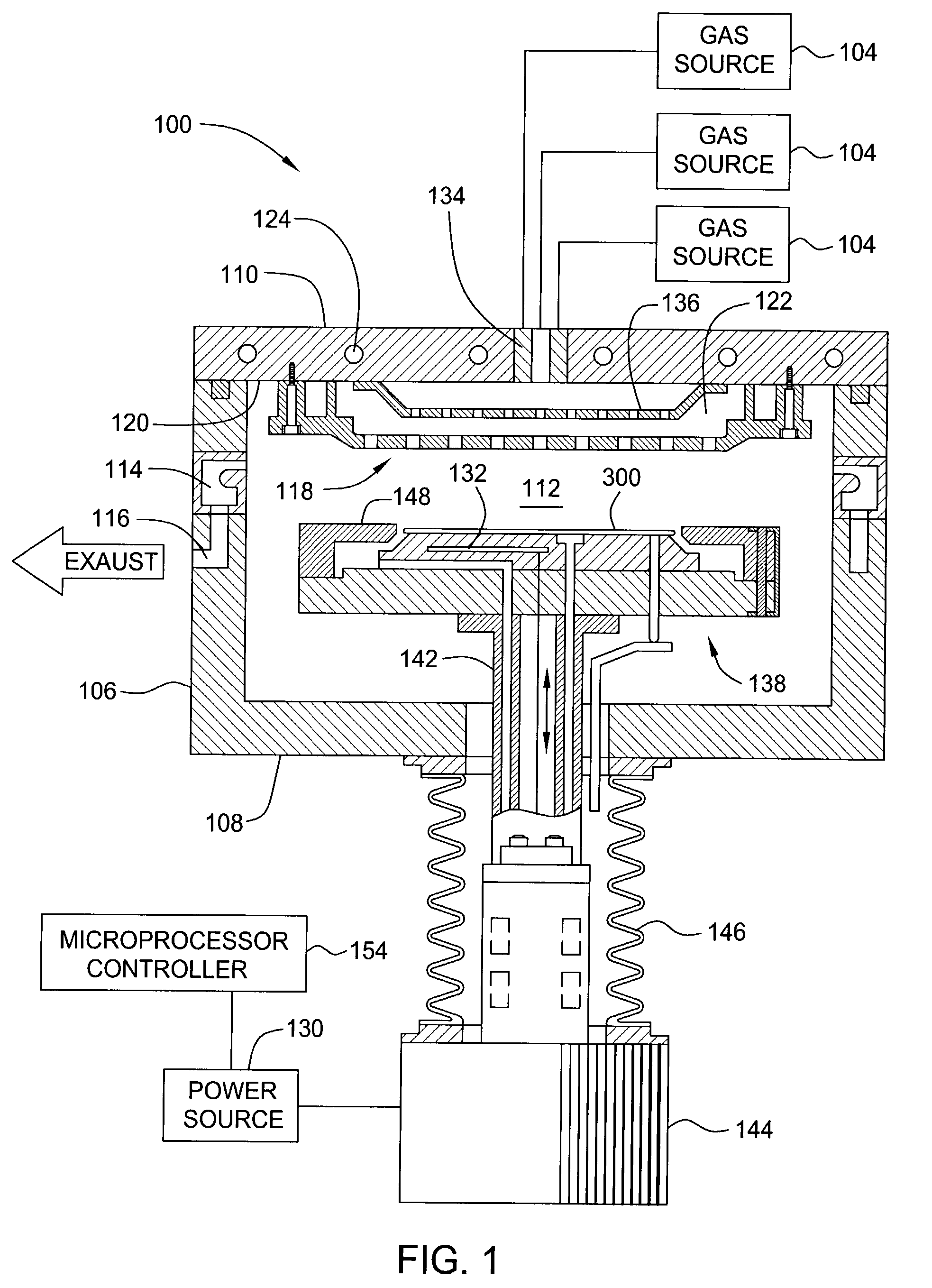
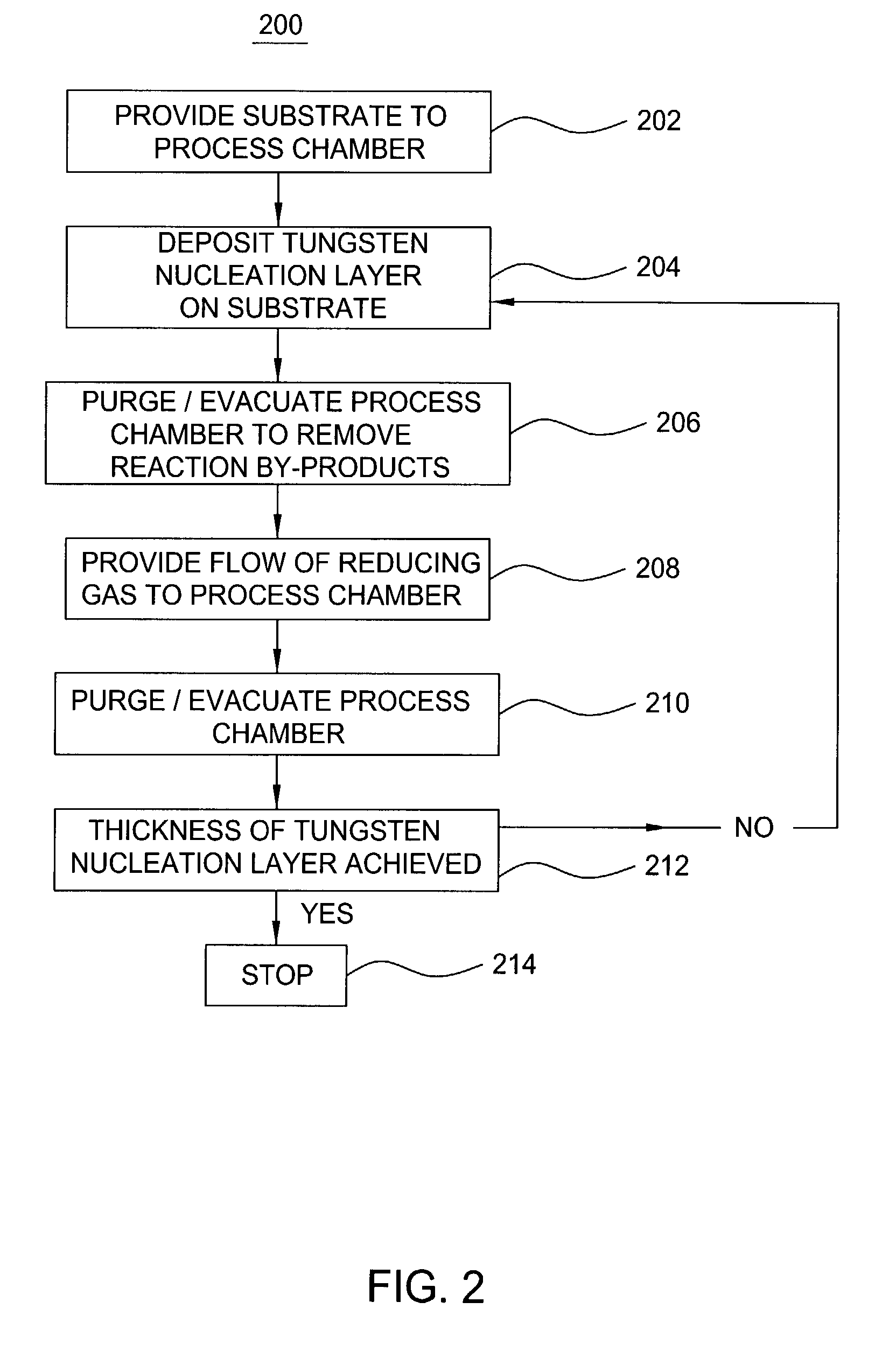
[0015]Embodiments described herein relate to a method for depositing a tungsten nucleation layer on a substrate. FIG. 1 depicts a schematic cross-sectional view of a chemical vapor deposition (CVD) process chamber 100 that may be used to practice embodiments of the invention described herein. The process chamber 100 may be part of a processing system (not shown) that includes multiple processing chambers connected to a central transfer chamber (not shown) and serviced by a robot (not shown).

[0016]The process chamber 100 includes walls 106, a bottom 108, and a lid 110 that define a process volume 112. The walls 106 and bottom 108 are typically fabricated from a unitary block of aluminum. The walls 106 may have conduits (not shown) therein through which a fluid may be passed to control the temperature of the walls 106. The process chamber 100 may also include a pumping ring 114 that couples the process volume 112 to an exhaust port 116 as well as other pumping components (not shown).

[...


PUM

PropertyMeasurementUnit
time periodaaaaaaaaaa
temperatureaaaaaaaaaa
total pressureaaaaaaaaaa

Abstract

A method of forming a tungsten nucleation layer using a sequential deposition process. The tungsten nucleation layer is formed by reacting pulses of a tungsten-containing precursor and a reducing gas in a process chamber to deposit tungsten on the substrate. Thereafter, reaction by-products generated from the tungsten deposition are removed from the process chamber. After the reaction by-products are removed from the process chamber, a flow of the reducing gas is provided to the process chamber to react with residual tungsten-containing precursor remaining therein. Such a deposition process forms tungsten nucleation layers having good step coverage. The sequential deposition process of reacting pulses of the tungsten-containing precursor and the reducing gas, removing reaction by-products, and than providing a flow of the reducing gas to the process chamber may be repeated until a desired thickness for the tungsten nucleation layer is formed.

Description

CROSS-REFERENCE TO RELATED APPLICATIONS[0001]The present application is a continuation-in-part of application Ser. No. 10 / 023,125, filed Dec. 17, 2001, entitled “Pulse Nucleation Enhanced Nucleation Technique For Improved Step Coverage and Better Gap Fill For WCVD Process,” which in turn claims priority from U.S. provisional application No. 60 / 305,307, filed Jul. 13, 2001, entitled “Pulse Nucleation Enhanced Nucleation Technique For Improved Step Coverage and Better Gap Fill For WCVD Process.” Each of these applications is incorporated herein by reference in its entirety.BACKGROUND OF THE INVENTION[0002]1. Field of the Invention[0003]The present invention generally relates to a method of forming tungsten layers and, more particularly forming tungsten layers using a pulsed nucleation deposition process.[0004]2. Description of the Related Art[0005]Integrated circuits have evolved into complex devices that can include millions of components (e.g., transistors, capacitors and resistors)...

Claims


Application Information

Patent Timeline
Patent Type & Authority Patents(United States)
IPC IPC(8): C30B25/16C23C16/14C23C16/44C23C16/455C30B25/02H01L21/285H01L21/768
CPCC23C16/14C23C16/45523C23C16/45525C30B25/02H01L21/28562C30B29/02
Inventor LU, XINLIANGJIAN, PINGYOO, JONG HYUNLAI, KEN KAUNGMAK, ALFRED W.JACKSON, ROBERT L.XI, MING
Owner APPLIED MATERIALS INC
Why Eureka
Try Eureka