Unlock instant, AI-driven research and patent intelligence for your innovation.
Semiconductor equipment
Inactive Publication Date: 2005-09-06
MX ENTERTAINMENT +1
View PDF6 Cites 19 Cited by
Summary
Abstract
Description
Claims
Application Information
AI Technical Summary
This helps you quickly interpret patents by identifying the three key elements:
Problems solved by technology
Method used
Benefits of technology
Benefits of technology
[0010]In the above equipment, the trench is disposed in the rear side of the substrate, and the second metal layer embedded in the trench provides the second electrode. Therefore, a current path between the first and second electrodes becomes short, so that the resistance between the first and second electrodes is reduced. Thus, an ON-state resistance between the first and second electrodes is also decreased, i.e., the vertical transistor has a low ON-state resistance.
[0030]In the above equipment, a current path between the first semiconductor layer and the source diffusion region becomes short, so that the resistance between them is reduced. Thus, an ON-state resistance between them is also decreased, i.e., the MOS transistor has a low ON-state resistance.
Problems solved by technology
Therefore, the manufacturing cost of the semiconductor equipment 200 becomes higher.
A resistance of the N+ type semiconductor layer in the V-DMOS becomes a rate-determining factor, so that it is difficult to reduce an ON-state resistance of the V-DMOS.
Method used
Image
Click on the blue label to locate the original text in one second.
Reading with bidirectional positioning of images and text.
Examples
first embodiment
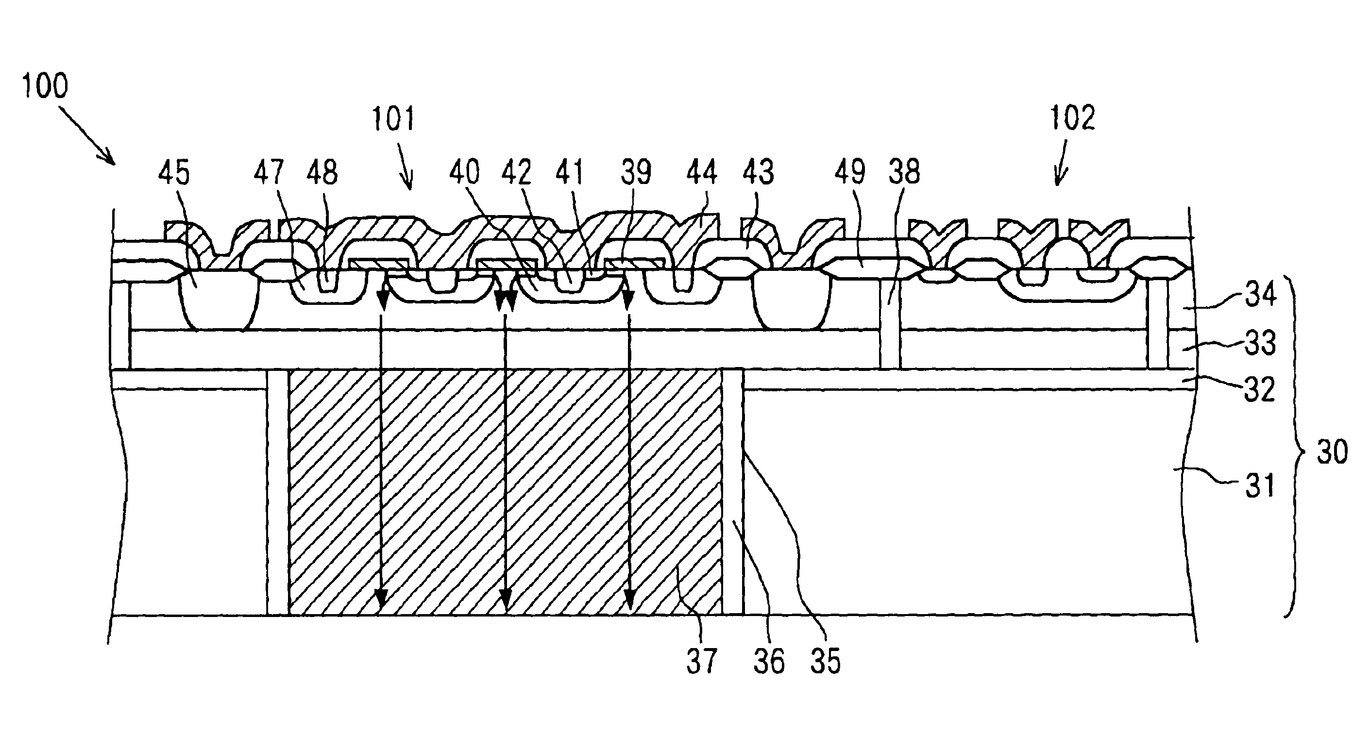
[0046](First Embodiment)
[0047]Semiconductor equipment 100 according to a first embodiment of the present invention is shown in FIG. 1. The semiconductor equipment 100 includes a vertical type MOS transistor 101 and a lateral type bipolar transistor 102 formed on a semiconductor substrate 30. The substrate 30 is an SOI substrate (i.e., a silicon on insulator substrate) embedding an insulation film 32 therein. The insulation film 32, an N+ type first semiconductor layer 33, and an N type second semiconductor layer 34 are formed on a silicon substrate (i.e., a Si substrate) 31 in this order. The first semiconductor layer 33 is an N+ type semiconductor, and the second semiconductor layer 34 is an N type semiconductor, a dope density of which is lower than that of the N+ type semiconductor.
[0048]A P type diffusion layer 40 is formed on a surface portion of the second semiconductor layer 34. Further, an N+ type diffusion layer 41 and a P+ type diffusion layer 42 are formed on a surface po...
second embodiment
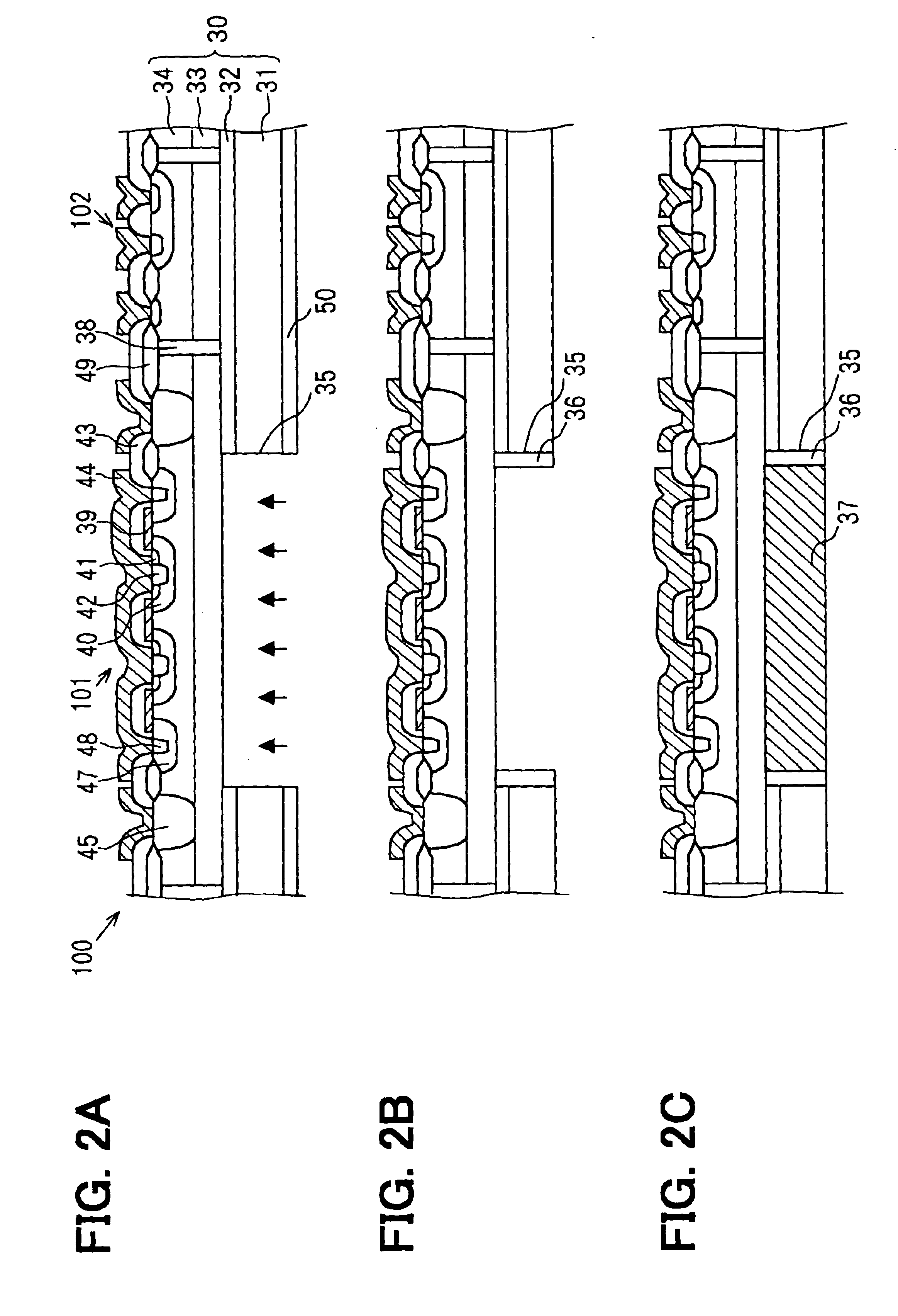
[0062](Second Embodiment)
[0063]Three semiconductor equipments 110, 120, 130 according to a second embodiment of the present embodiment are shown in FIGS. 3-5, respectively.
[0064]In a vertical type MOS transistor 111 of the semiconductor equipment 110 shown in FIG. 3, the trench 35 is formed on the rear side of the substrate 30, and disposed under the insulation film 32. The trench 35 is disposed perpendicularly to the surface of the substrate 30. Comparing with the semiconductor equipment 100 shown in FIG. 1, no sidewall insulation film is formed on the sidewall of the trench 35 shown in FIG. 3, so that the metal layer 37 embedded in the trench 35 is not isolated and separated from surroundings.
[0065]When only one MOS transistor 111 is formed on the substrate 30, or when a plurality of vertical type MOS transistors 111 having the same drain potential is formed on the substrate 30, the semiconductor equipment 110 having no sidewall insulation film can be used for them. In this case, ...
third embodiment
[0069](Third Embodiment)
[0070]Semiconductor equipment 140 according to a third embodiment of the present invention is shown in FIG. 6. In a vertical type MOS transistor 141 of the semiconductor equipment 140, a P type diffusion region 40A is disposed on the surface portion of the second semiconductor layer 34. Further, an N+ type diffusion region 41A is disposed on the surface portion of the diffusion region 40A. A gate electrode 39A penetrates the diffusion region 40A, and reaches the second semiconductor layer 34. The gate electrode 39A contacts the diffusion regions 40A, 41A and the second semiconductor layer 34 through a gate insulation film (not shown).
[0071]As shown as arrows in FIG. 6, electrons are outputted from the diffusion region 41A as a source, pass through the diffusion region 40A as a channel and the first semiconductor layer 33 as a drain straightly, and are collected into the metal layer 37. Therefore, the current path between the source and the drain becomes short...
PUM
Abstract
Semiconductor equipment includes a semiconductor substrate with a semiconductor layer embedded therein and a vertical type transistor. The substrate has a principal side, a rear side opposite to the principal side, and a trench disposed in the rear side of the substrate. The vertical type transistor has a first electrode disposed in the principal side of the substrate, a second electrode disposed in the rear side, and a diffusion region disposed in the principal side. The first electrode connects to the diffusion region through an interlayer insulation film. The second electrode is disposed in the trench and connects to the semiconductor layer exposed in the trench. This vertical transistor has a low ON-state resistance.
Description
CROSS REFERENCE TO RELATED APPLICATION[0001]This application is based on Japanese Patent Applications No. 2002-273117 filed on Sep. 19, 2002, and No. 2003-307286 filed on Aug. 29, 2003, the disclosures of which are incorporated herein by reference.FIELD OF THE INVENTION[0002]The present invention relates to semiconductor equipment, specifically, the present invention relates to semiconductor equipment having a low ON-state resistance transistor.BACKGROUND OF THE INVENTION[0003]Semiconductor equipment 200 having a metaloxide semiconductor transistor (i.e., a MOS transistor) according to a prior art is disclosed in Japanese Patent No. 3257057-B2 (Japanese Unexamined Patent Application Publication No. H05-198758). As shown in FIG. 14, the semiconductor equipment 200 includes a semiconductor substrate 3. An insulation layer 4 having a box shape (i.e., a box type insulation layer) is disposed in the substrate 3. The insulation layer 4 has three openings for opening upside of the substra...
Claims
Application Information
Patent Timeline
Application Date:The date an application was filed.
Publication Date:The date a patent or application was officially published.
First Publication Date:The earliest publication date of a patent with the same application number.
Issue Date:Publication date of the patent grant document.
PCT Entry Date:The Entry date of PCT National Phase.
Estimated Expiry Date:The statutory expiry date of a patent right according to the Patent Law, and it is the longest term of protection that the patent right can achieve without the termination of the patent right due to other reasons(Term extension factor has been taken into account ).
Invalid Date:Actual expiry date is based on effective date or publication date of legal transaction data of invalid patent.
