Eureka AIR delivers breakthrough ideas for toughest innovation challenges, trusted by R&D personnel around the world.

Architecture for mask programmable devices

Inactive Publication Date: 2005-09-13
AVAGO TECH WIRELESS IP SINGAPORE PTE
View PDF2 Cites 5 Cited by
  • Summary
  • Abstract
  • Description
  • Claims
  • Application Information

AI Technical Summary

Benefits of technology

[0007]Accordingly, the present invention is directed to a semi-programmable ASIC using two metals for the metal layers. The semi-programmable ASIC may have a prefabricated first section and a customized second section. The prefabricated first section and the customized second section may each include one or more metal layers. The one or more metal layers included in the prefabricated first section may be used to define undifferentiated sets of electrical and logic elements. An undifferentiated set of electrical and logic element

Problems solved by technology

Unfortunately, copper may be difficult to etch in such a process.
However, the copper process may cost significantly more than the traditional aluminum process.

Method used


Image

  • Architecture for mask programmable devices
  • Architecture for mask programmable devices
  • Architecture for mask programmable devices

Examples


Embodiment Construction

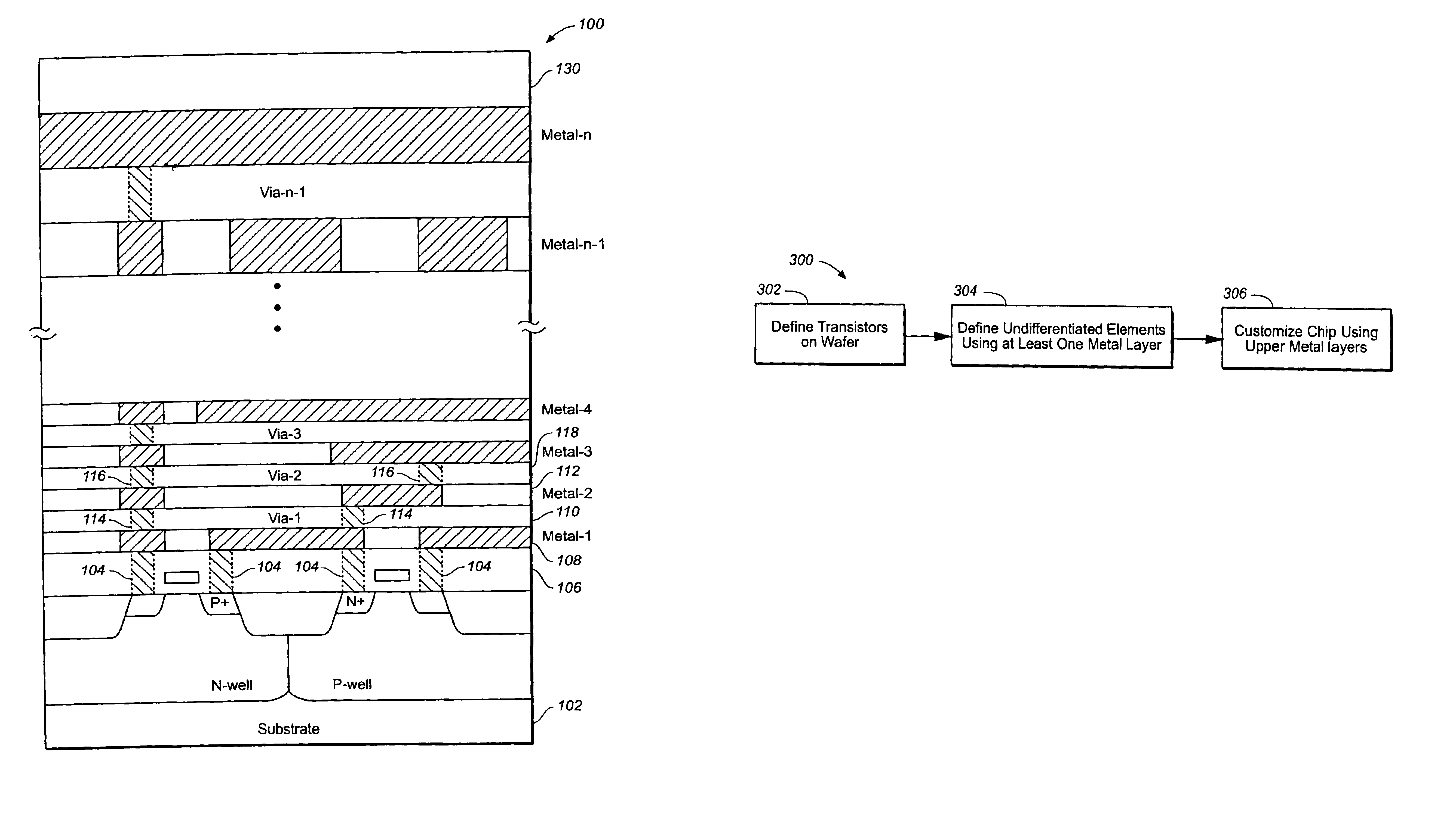
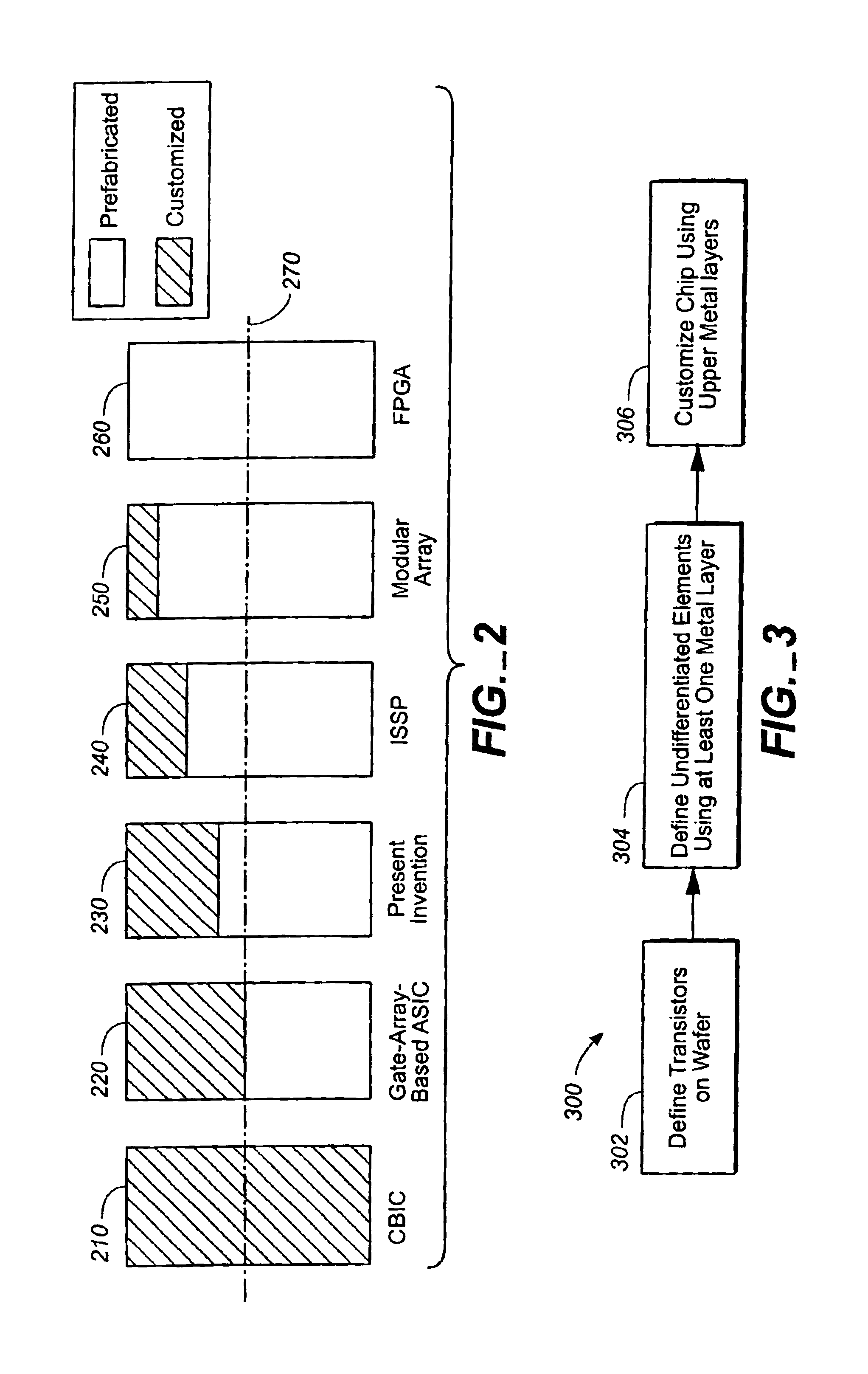
[0017]Reference will now be made in detail to the presently preferred embodiments of the invention, examples of which are illustrated in the accompanying drawings.

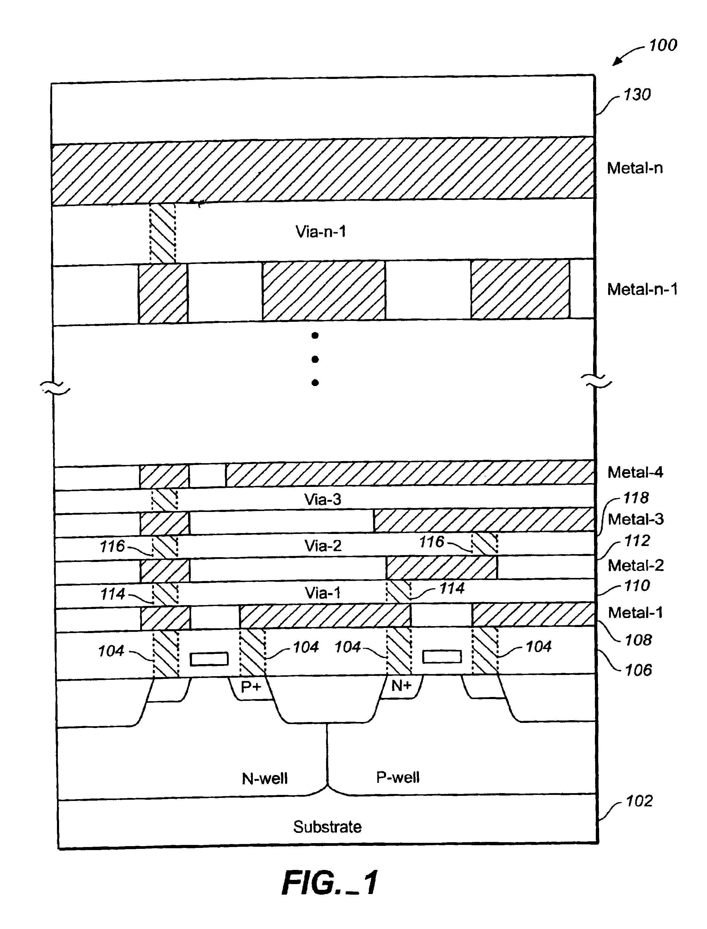
[0018]Referring first to FIG. 1, a schematic diagram illustrating a partial cross-sectional view of an exemplary ASIC 100 in which the present invention may be implemented is shown. The ASIC 100 may be formed on a semiconductor substrate 102. Those of ordinary skill in the art will understand that a number of masks may be used to form transistors which are the building block of logic gates. Such masks may include masks for forming buried layers and isolation (e.g., well structures), base diffusion, and emitter diffusion, masks for patterning gate electrodes, and the like. FIG. 1 shows two of such transistors.

[0019]After the transistors are formed, a contact layer 106 may be formed on top of the transistors by growth or deposition of insulating material. Contact holes 104 within the contact layer 106 may then be formed and ...


PUM


Abstract

The present invention is directed to a semi-programmable ASIC using two metals for the metal layers. The semi-programmable ASIC may have a prefabricated first section and a customized second section. The prefabricated first section and the customized second section may each include one or more metal layers. The one or more metal layers included in the prefabricated first section may be used to define undifferentiated sets of electrical and logic elements. An undifferentiated set of electrical and logic elements may be a NAND logic gate, a NOR logic gate, or the like. The one or more metal layers included in the customized second section may be used to define logic functions of the undifferentiated sets of electrical and logic elements. The metal used in the one or more metal layers included in the prefabricated first section may be of one type such as copper, copper alloy, or the like, and the metal used in the metal layers included in the customized second section may be of another type such as aluminum, aluminum alloy, or the like.

Description

FIELD OF THE INVENTION[0001]This invention relates generally to integrated circuits, and particularly to architecture for mask programmable devices.BACKGROUND OF THE INVENTION[0002]ICs (integrated circuits) are generally made on a thin and circular silicon wafer. The transistors and wiring of an IC are conventionally made from many mask layers built on top of one another. Each successive mask layer may have a pattern that is defined using a mask. A mask is the shape used for processing features in a particular process step of integrated circuit production. When a mask layer is defined using a mask chosen or provided by a customer, the mask layer is programmed or customized.[0003]An ASIC (application specific integrated circuit) is an IC designed specifically for a particular application or use. There are three categories of ASICs in terms of programmability of mask layers: fully programmable ASICs, non-programmable ASICs, and semi-programmable ASICs. In a fully programmable ASIC, al...

Claims


Application Information

Patent Timeline
IPC IPC(8): H01L29/66H01L29/76H01L23/48H01L31/06H01L27/10H01L31/062H01L29/94H01L31/101H01L31/113H01L31/119H01L31/115H01L27/02H01L27/118
CPCH01L27/0207H01L27/11803H01L27/11807
Inventor CORRIGAN, WILFRED
Owner AVAGO TECH WIRELESS IP SINGAPORE PTE
Why Eureka
Eureka Blog
Learn More