Programmable logic device

a logic device and programmable technology, applied in the direction of logic circuits using specific components, power consumption reduction, pulse techniques, etc., can solve the problems of increased power consumption, increased circuit area, and significant increase in the number of elements in the entire pld, and achieve short startup time and low power consumption

Inactive Publication Date: 2013-11-07
SEMICON ENERGY LAB CO LTD
View PDF2 Cites 61 Cited by
  • Summary
  • Abstract
  • Description
  • Claims
  • Application Information

AI Technical Summary

Benefits of technology

[0021]According to one embodiment of the present invention, it is possible to provide a low power consumption PLD that achieves high-speed configuration capable of dynamic configuration and has short startup time.
[0022]Moreover, it is possible to provide a PLD that has a smaller number of transistors or a smaller circuit area than a PLD using an SRAM as a configuration memory.

Problems solved by technology

However, with the structure disclosed in Patent Document 1, regular refresh operation is required to maintain configuration data in the DRAM, and the power consumption is increased as a result.
In the case where an SRAM is used as the configuration memory, at least four transistors are required, which leads to a significant increase in the number of elements in the entire PLD and an increase in the circuit area.

Method used


Image

  • Programmable logic device
  • Programmable logic device
  • Programmable logic device

Examples


embodiment 1

[0045]In Embodiment 1, one embodiment of a PLD will be described with reference to FIGS. 1A and 1B, FIG. 2, FIG. 3, and FIG. 4.

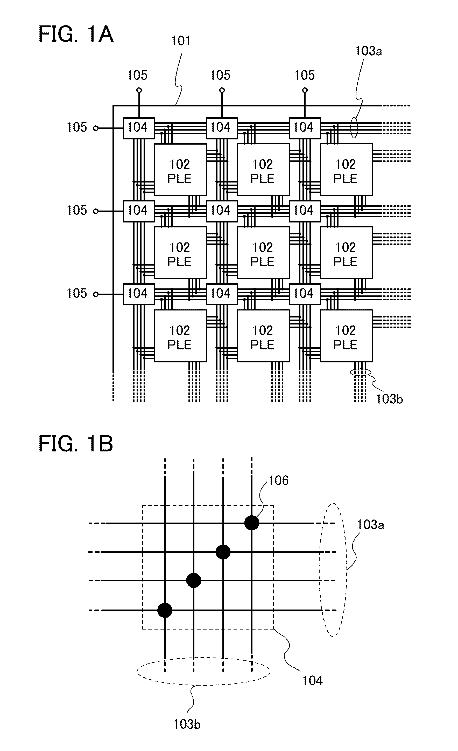
[0046]FIG. 1A conceptually illustrates part of a logic array in the PLD. A logic array 101 includes a plurality of programmable logic elements 102 arranged in an array (the programmable logic element is denoted by PLE in FIG. 1A). Here, the term “arranged in an array” means that the programmable logic elements are arranged at regular intervals, and the arrangement is not limited to that illustrated in FIG. 1A.

[0047]A plurality of wirings are formed to surround the programmable logic elements 102. In FIG. 1A, these wirings consist of a plurality of horizontal wiring groups 103a and a plurality of vertical wiring groups 103b. A wiring group is a bundle of wirings, and for example is a bundle of four wirings as illustrated in FIG. 1A. A switch box 104 is provided at an intersection of the horizontal wiring group 103a and the vertical wiring group 103b. The hori...

embodiment 2

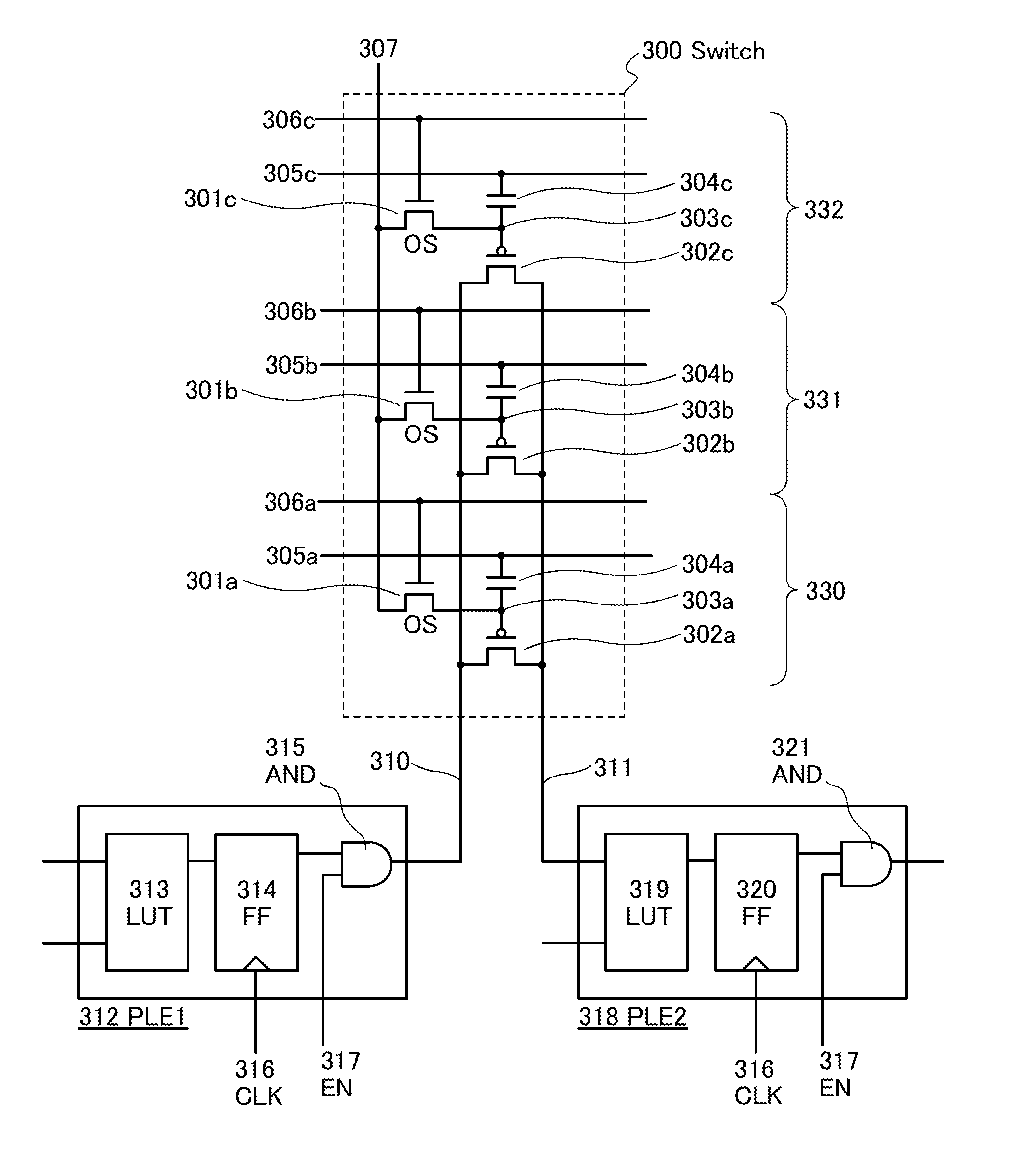
[0082]In Embodiment 2, a switch 300 in which the n-channel second transistors used in the switch 200 shown in Embodiment 1 are replaced with p-channel second transistors will be described with reference to FIG. 5 and FIG. 6.

(Structure of Switch 300)

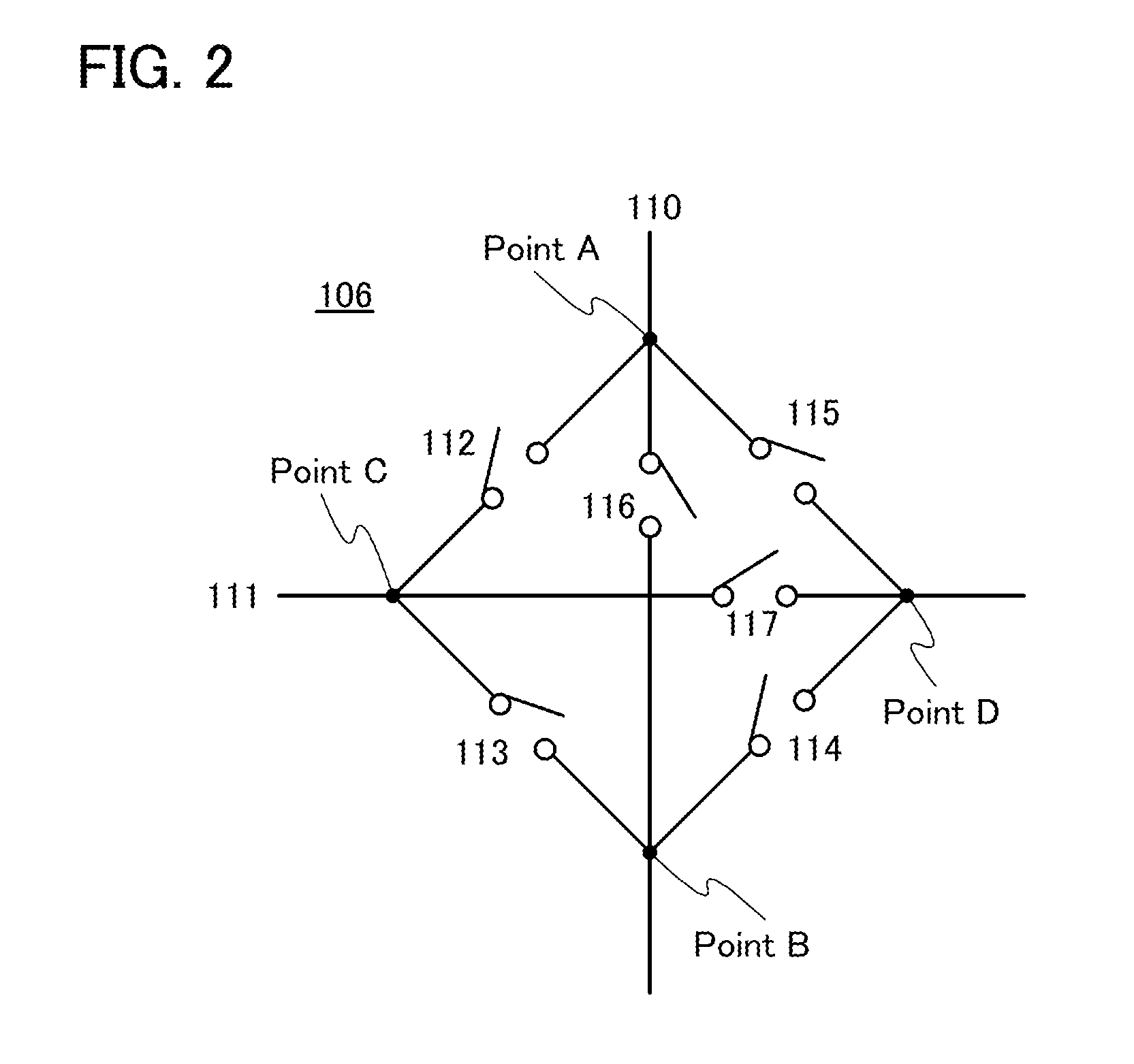
[0083]FIG. 5 illustrates the switch 300 in this embodiment. The switch 300 corresponds to each of the switches 112 to 117 in FIG. 2 and its structure is the same as that of the switch 200 described in Embodiment 1 except that the n-channel second transistors 202a to 202c are replaced with transistors with opposite polarity, that is, p-channel second transistors 302a to 302c.

[0084]The switch 300 controls connection between a programmable logic element 312 and a programmable logic element 318 in a PLD. Each of the programmable logic elements 312 and 318 corresponds to one of the plurality of programmable logic elements 102 in FIG. 1. For example, in FIG. 5, the programmable logic element 312 can be composed of a lookup table 313, a flip-fl...

embodiment 3

[0112]Embodiment 1 shows the switch 200 using three groups each including a first transistor, a second transistor, and a capacitor, whereas Embodiment 3 will explain a switch 400 including at least three groups (hereinafter referred to as N groups, where N is an integer of 3 or more) of these elements with reference to FIG. 7.

[0113]The switch 400 corresponds to each of the switches 112 to 117 in FIG. 2 and controls connection between a programmable logic element 412 and a programmable logic element 418 in a PLD. Each of the programmable logic elements 412 and 418 corresponds to one of the plurality of programmable logic elements 102 in FIG. 1. For example, in FIG. 7, the programmable logic element 412 can be composed of a lookup table 413, a flip-flop 414, and an AND circuit 415, and the programmable logic element 418 can be composed of a lookup table 419, a flip-flop 420, and an AND circuit 421.

[0114]As in the switch 200 described in Embodiment 1, the first transistor in the switch...


PUM


Abstract

Disclosed is a programmable logic device (PLD) which can undergo dynamic configuration at a high speed. The PLD includes a plurality of programmable logic elements (PLEs) and a switch for selecting electrical connection between the PLEs. The switch includes a plurality of circuit groups each of which includes first and second transistors. The second transistors of the circuit groups are electrically connected in parallel with one another. In each of the circuit groups, the electrical conduction between a source and a drain of the second transistor is determined based on configuration data held at a node between the gate of the second transistor and a drain of the first transistor, which allows the selection of the electrical connection and disconnection between the programmable logic elements by the selection of one of the circuit groups.

Description

TECHNICAL FIELD[0001]The present invention relates to a semiconductor device and particularly to a programmable logic device and a semiconductor device including the programmable logic device. The present invention also relates to an electronic device including the semiconductor device.BACKGROUND ART[0002]Unlike a normal integrated circuit in which all circuits are fixed at the time of manufacture, a programmable logic device (PLD) is a device that can function with an intended circuit structure set by a user at the time of actual use after shipment. Examples of such devices that are programmable by users are a small-scale programmable array logic (PAL) and generic array logic (GAL) and a large-scale complex programmable logic device (CPLD) and field programmable gate array (FPGA); in this specification, such devices are collectively called a programmable logic device (hereinafter referred to as PLD).[0003]PLDs have advantages such as a short development period and flexibility in ch...

Claims


Application Information

Patent Timeline
Patent Type & Authority Applications(United States)
IPC IPC(8): H03K19/094
CPCH03K19/094H01L27/0688H01L27/11803H03K19/0013H03K19/17744H01L27/1225H10B41/70
Inventor KUROKAWA, YOSHIYUKI
Owner SEMICON ENERGY LAB CO LTD
Why Eureka
Try Eureka