Multi-metal layer MEMS structure and process for making the same

a technology of metal layer and mems, applied in the field of microelectromechanical system (mems) devices, can solve problems such as structure bending or premature failur

Inactive Publication Date: 2005-09-13
AKUSTICA
View PDF21 Cites 57 Cited by
  • Summary
  • Abstract
  • Description
  • Claims
  • Application Information

AI Technical Summary

Problems solved by technology

When devices are comprised of composite structures, the different materials comprising the composite structure respond to thermal and other types of stress differently, which may cause the structure to bend or fail prematurely.

Method used


Image

  • Multi-metal layer MEMS structure and process for making the same
  • Multi-metal layer MEMS structure and process for making the same
  • Multi-metal layer MEMS structure and process for making the same

Examples


Embodiment Construction

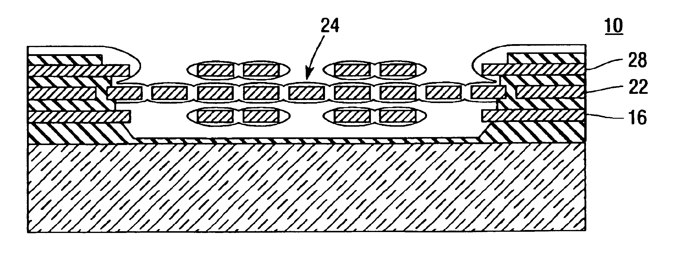
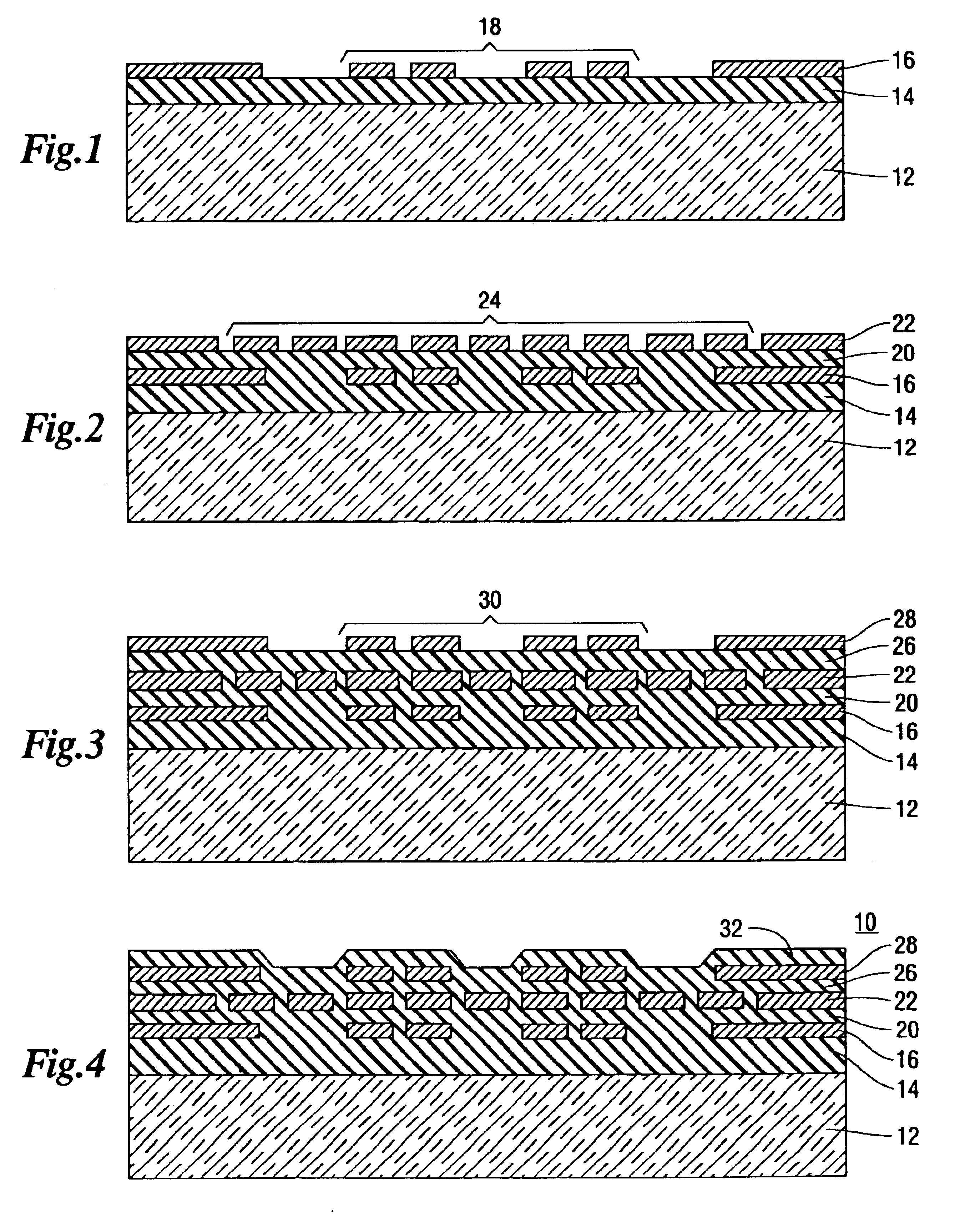
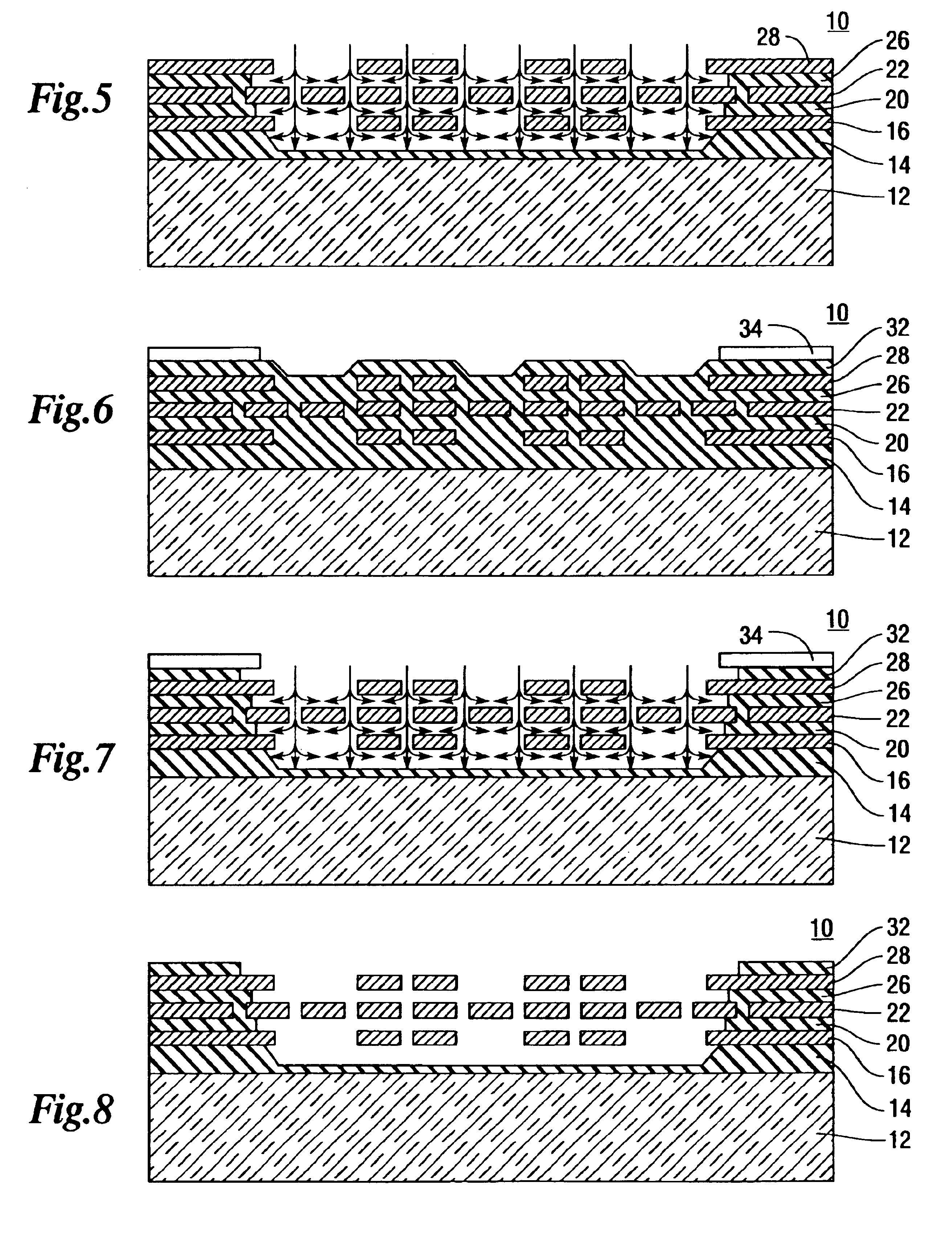
[0023]FIGS. 1-4 illustrate a process in which a multi-layer structure 10 (see FIG. 4) is constructed by forming alternating layers of sacrificial material and metal on a substrate. “Forming” as used herein is intended to be used in its broadest sense of using any type of CMOS process, e.g. chemical vapor deposition, sputtering, etc. to deposit, form or otherwise create a layer of material. Also, references herein to a first layer of metal, a second layer of metal, etc. need not correspond to metal one, metal two, etc. The first layer of metal may be implemented in, for example, metal two. The substrate may be, for example, a silicon substrate 12 typically used in CMOS manufacturing processes. As seen in FIG. 1, a base layer of sacrificial material 14 may be formed on the substrate 12. The sacrificial layer 14 may be any of a variety of materials that may be dry etched with an etchant to which the silicon substrate 12 is impervious. For example, dielectrics such as silicon dioxide, f...


PUM

PropertyMeasurementUnit
thicknessaaaaaaaaaa
stressaaaaaaaaaa
structureaaaaaaaaaa

Abstract

The present invention is directed to a structure comprised of alternating layers of metal and sacrificial material built up using standard CMOS processing techniques, a process for building such a structure, a process for fabricating devices from such a structure, and the devices fabricated from such a structure. In one embodiment, a first metal layer is carried by a substrate. A first sacrificial layer is carried by the first metal layer. A second metal layer is carried by the sacrificial layer. The second metal layer has a portion forming a micro-machined metal mesh. When the portion of the first sacrificial layer in the area of the micro-machined metal mesh is removed, the micro-machined metal mesh is released and suspended above the first metal layer a height determined by the thickness of the first sacrificial layer. The structure may be varied by providing a base layer of sacrificial material between the surface of the substrate and the first metal layer. In that manner, a portion of the first metal layer may form a micro-machined mesh which is released when a portion of the base sacrificial layer in the area of the micro-machined mesh is removed. Additionally, a second layer of sacrificial material and a third metal layer may be provided. A micro-machined mesh may be formed in a portion of the third metal layer. The structure of the present invention may be used to construct variable capacitors, switches and, when certain of the meshes are sealed, microspeakers and microphones.

Description

BACKGROUND OF THE INVENTION[0001]The present invention is directed generally to micro-electromechanical system (MEMS) devices and, more particularly, to MEMS devices constructed from alternating layers of metal and a sacrificial material.[0002]MEMS devices are typically constructed using traditional CMOS processing techniques. Such processing techniques are well developed as they are used to fabricate many different types of integrated circuits such as memory devices, processors, logic circuits, to name a few. As a result, the construction of MEMS devices is advanced whenever there are improvements in CMOS processing techniques.[0003]In fabricating a typical MEMS device, various layers of material are formed on a substrate and etched according to a pattern to form the desired device(s). The resulting device is typically formed of a composite of various layers of materials. The device is then released from the substrate by removing a portion of the substrate from under the device. ME...

Claims


Application Information

Patent Timeline
Patent Type & Authority Patents(United States)
IPC IPC(8): B81B3/00B81C1/00C23F1/00H01G4/00H01G9/00H01G7/00H01G5/00H01G13/00H01L23/48H01L23/52H04R19/04H04R19/02H04R19/00H04R31/00H01H59/00
CPCB81C1/00158H01G5/16B81B2201/018B81B2201/0257B81C2201/0109
Inventor GABRIEL, KAIGHAM J.ZHU, XU
Owner AKUSTICA
Why Eureka
Try Eureka