Semiconductor integrated circuit device in which operating frequency, supply voltage and substrate bias voltage are controllable to reduce power consumption

a technology of integrated circuit and integrated circuit device, which is applied in the direction of pulse generator, pulse technique, instruments, etc., can solve the problems of degrading circuit performance, increasing power consumption, and accordingly increasing power consumption, so as to prolong battery life, improve power consumption, and improve power consumption

Inactive Publication Date: 2005-09-13
RENESAS ELECTRONICS CORP
View PDF3 Cites 43 Cited by
  • Summary
  • Abstract
  • Description
  • Claims
  • Application Information

AI Technical Summary

Benefits of technology

[0016]The main circuit is divided into two or more blocks, in each of which blocks the clock frequency, the supply voltage and the substrate bias are controlled so that the most approximate performance may be achieved. This makes it possible for the main circuit to operate on the operating characteristics according to the processing load to be done by each block, for realizing more minute control.
[0017]Further, the system arranged to use the foregoing semiconductor integrated circuit device is disclosed. In the system including the semiconductor integrated circuit device, the battery, and the voltage converting circuit, th

Problems solved by technology

In actuality, however, with improvement of an operating speed of the CMOS circuit, the power consumption is increased accordingly.
The increase of the power consumption gives rise to disadvantages of degrading the circuit performance and bringing about an erroneous operation.
The heat caused by the increase of the power consumption has the adverse effect on the mount of the semiconductor integrated circuit device, which dis

Method used


Image

  • Semiconductor integrated circuit device in which operating frequency, supply voltage and substrate bias voltage are controllable to reduce power consumption
  • Semiconductor integrated circuit device in which operating frequency, supply voltage and substrate bias voltage are controllable to reduce power consumption
  • Semiconductor integrated circuit device in which operating frequency, supply voltage and substrate bias voltage are controllable to reduce power consumption

Examples


Embodiment Construction

[0045]Hereafter, the description will be oriented to an embodiment of the present invention with reference to the appended drawings.

[0046]FIG. 1 shows an embodiment of the present invention.

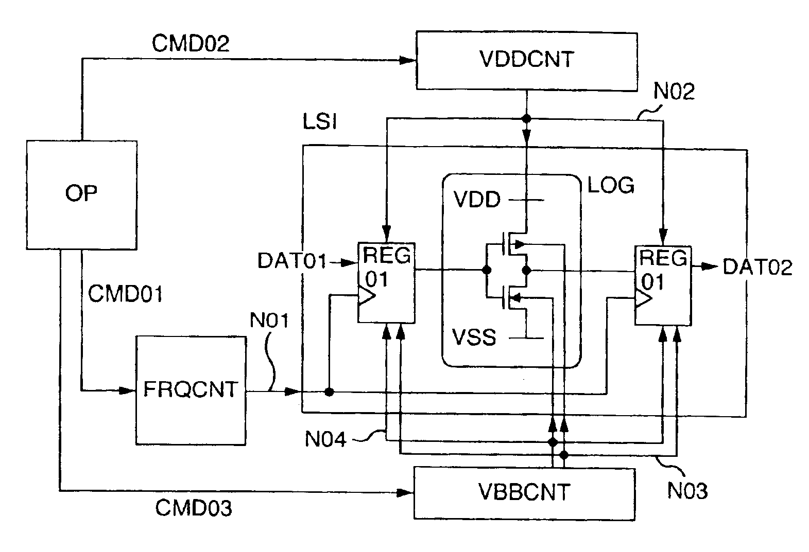
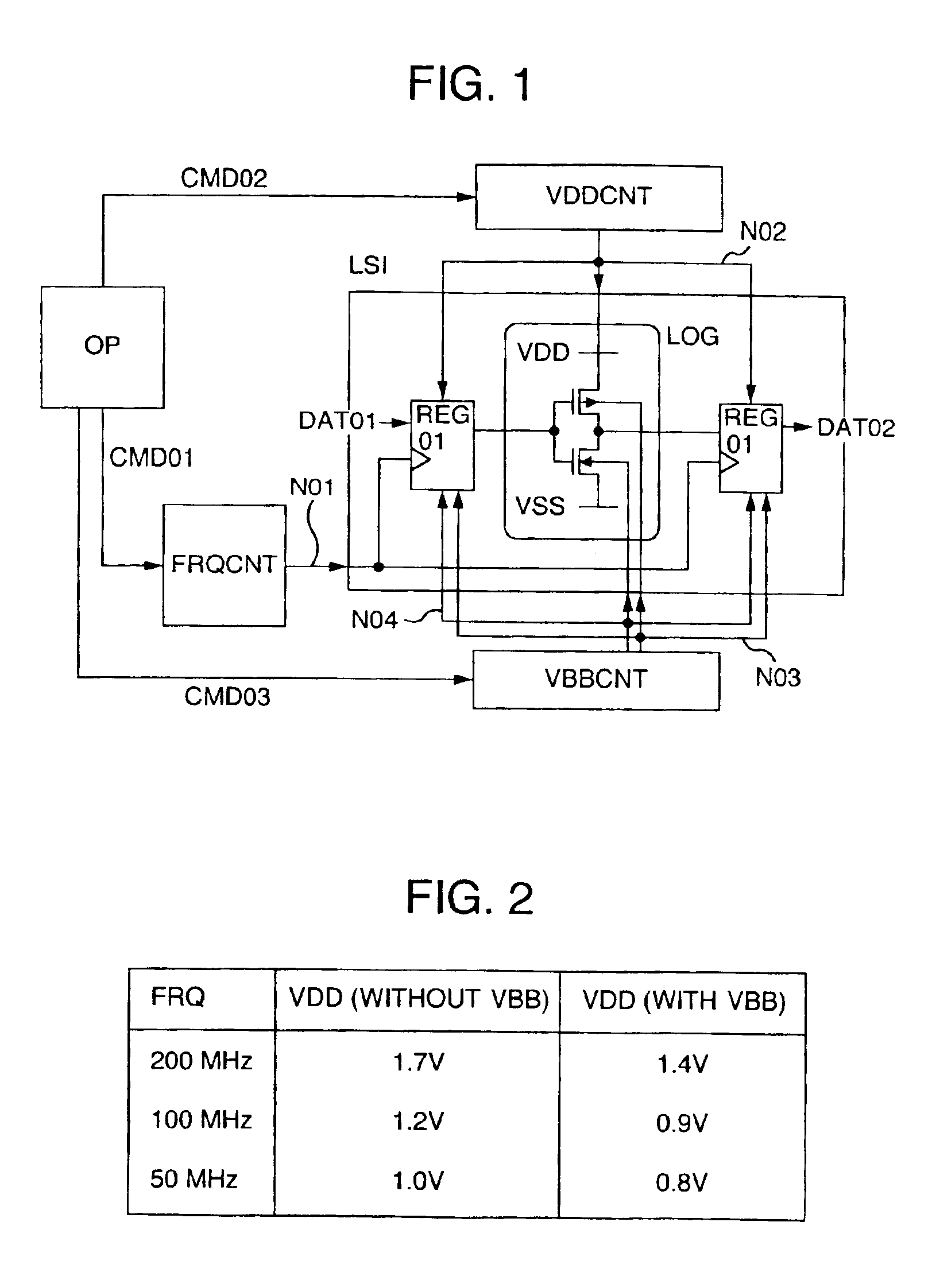
[0047]The semiconductor integrated circuit device of this embodiment includes a main circuit LSI that is a semiconductor integrated circuit such as a microprocessor composed of a CMOS circuit, a command generating circuit OP, a clock frequency controlling circuit FRQCNT, a power supply controlling circuit VDDCNT, and a substrate bias controlling circuit VBBCNT. The command generating circuit OP is served to output command signals CMD01, CMD02 and CMD03. The clock frequency controlling circuit FRQCNT is supplied with the command signal CMD01 and generates a clock signal having the corresponding frequency therewith as N01. The power supply controlling circuit VDDCNT is supplied with the command signal CMD02 and generates the corresponding supply voltage therewith as N02. The substrate bias controll...


PUM


Abstract

A semiconductor integrated circuit device includes control circuits FRQCNT, VDDCNT and VBBCNT that generate the optimum clock signal, supply voltage and substrate bias respectively and then supply them to a main circuit LSI. This operation makes it possible to suppress the variations of a CMOS circuit characteristic, thereby improving the circuit performance. Further, the low power consumption is realized without degrading the operating speed of the CMOS circuit or increasing the power consumption of the CMOS circuit.

Description

CROSS-REFERENCE TO RELATED APPLICATIONS[0001]This is a Continuation application of Ser. No. 09 / 811,387 filed Mar. 20, 2001 now U.S. Pat. No. 6,774,705, the entire disclosure of which is hereby incorporated by reference.BACKGROUND OF THE INVENTION[0002]The present invention relates to a semiconductor integrated circuit device, and more particularly to a semiconductor integrated circuit device which may be operated at both high speed and low electric power.[0003]In order to improve the performance of semiconductor integrated circuit devices composed of CMOS circuits, some methods have been proposed such as shrinkage of MOS transistors that are a components of the CMOS circuitry, lowering of absolute values of threshold voltages of the MOS transistors, and raising of a supply voltage. In actuality, however, with improvement of an operating speed of the CMOS circuit, the power consumption is increased accordingly. For example, as the threshold voltage of the MOS transistor is made lower...

Claims


Application Information

Patent Timeline
IPC IPC(8): H03K19/003H01L27/04G11C11/407H01L21/822H01L21/8234H01L27/088H03K19/00H03K19/094H03K19/0948H03K19/096
CPCH03K19/00384
Inventor MIYAZAKI, MASAYUKIISHIBASHI, KOICHIRO
Owner RENESAS ELECTRONICS CORP
Why Eureka
Try Eureka