Non-volatile NOR-type CAM memory

a cam memory, non-volatile technology, applied in the field of semi-conductor memories, can solve the problems of loss of binary content, difficult detection of non-matches during search, disassembly power, etc., to simplify the circuit structure of memory, simplify the cancellation algorithm, and simplify the search operation.

Active Publication Date: 2005-09-13
STMICROELECTRONICS SRL
View PDF5 Cites 7 Cited by
  • Summary
  • Abstract
  • Description
  • Claims
  • Application Information

AI Technical Summary

Benefits of technology

[0018]The disclosed embodiments of the present invention are directed to resolving the problems of the known CAM memory described hereinabove and, more particularly, to avoid the limitation imposed on the low threshold voltage of the transistors in order to simplify the cancellation algorithm, render the search operation more rapid and to simplify the circuit structure of the memory.
[0021]As will be readily appreciated from the foregoing, the memory, memory cell, and method of the present invention will have application in memories used in microprocessors, computers, computing systems, ASICs, and the like where CAM memories are used to redirect data from defective memory cells. The present invention avoids the limitation imposed on low threshold voltage of field effect transistors in order to simplify the cancellation process and to simplify and speed up the memory.

Problems solved by technology

CAM cells, irrespective of whether they are made with SRAMs or DRAMs, are relatively fast, but their binary content is lost as soon as the supply voltage is switched off.
If several cells in the same row conduct such parasitic currents, the voltage of the match line will not be sufficiently different from its initial pre-charge value (for example, VCC), so that, in a limited case, it may become difficult to detect a non-match during the search.
There still remains the problem of dissipating the power due to the parasite currents.
However, the addition of the of the recovery circuits complicates the circuit structure of the known memory described above.

Method used


Image

  • Non-volatile NOR-type CAM memory
  • Non-volatile NOR-type CAM memory
  • Non-volatile NOR-type CAM memory

Examples


Embodiment Construction

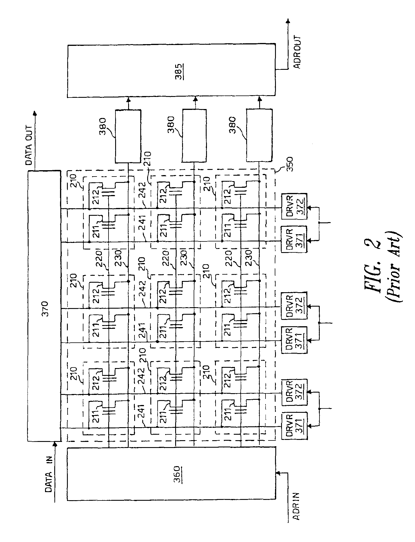
[0027]As can be seen in FIG. 3, the memory in accordance with the invention comprises a multiplicity of cells CELL ordered in a matrix of m rows and n columns. Each row of the matrix comprises four electric lines, respectively a word line WL1-m, a match line ML1-m, a ground line GL1-m, and a ground control line GNDCTRL1-m, which are connected to a block 10 performing the function of row decoder. Each column comprises two lines, a right-hand bit line BLR1-n and a left-hand bit line BLL1-n, connected to a block 11 performing the function of column decoder and a block 12 performing the function of controlling the search operation. All the cells in the same row are connected to the four lines associated with the row and all the cells in the same column are connected to the two lines associated with the column.

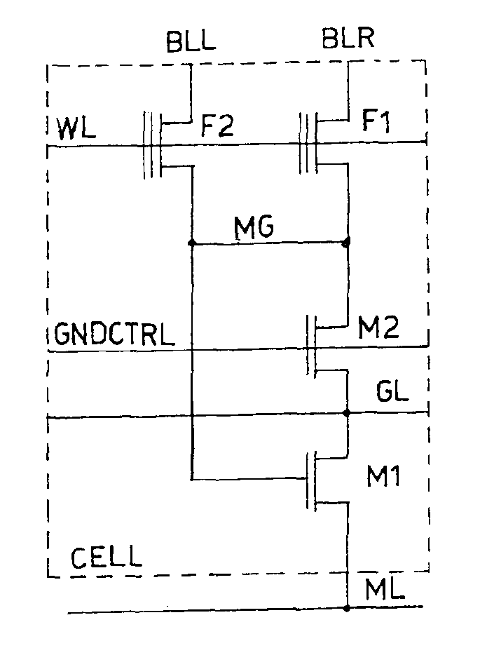
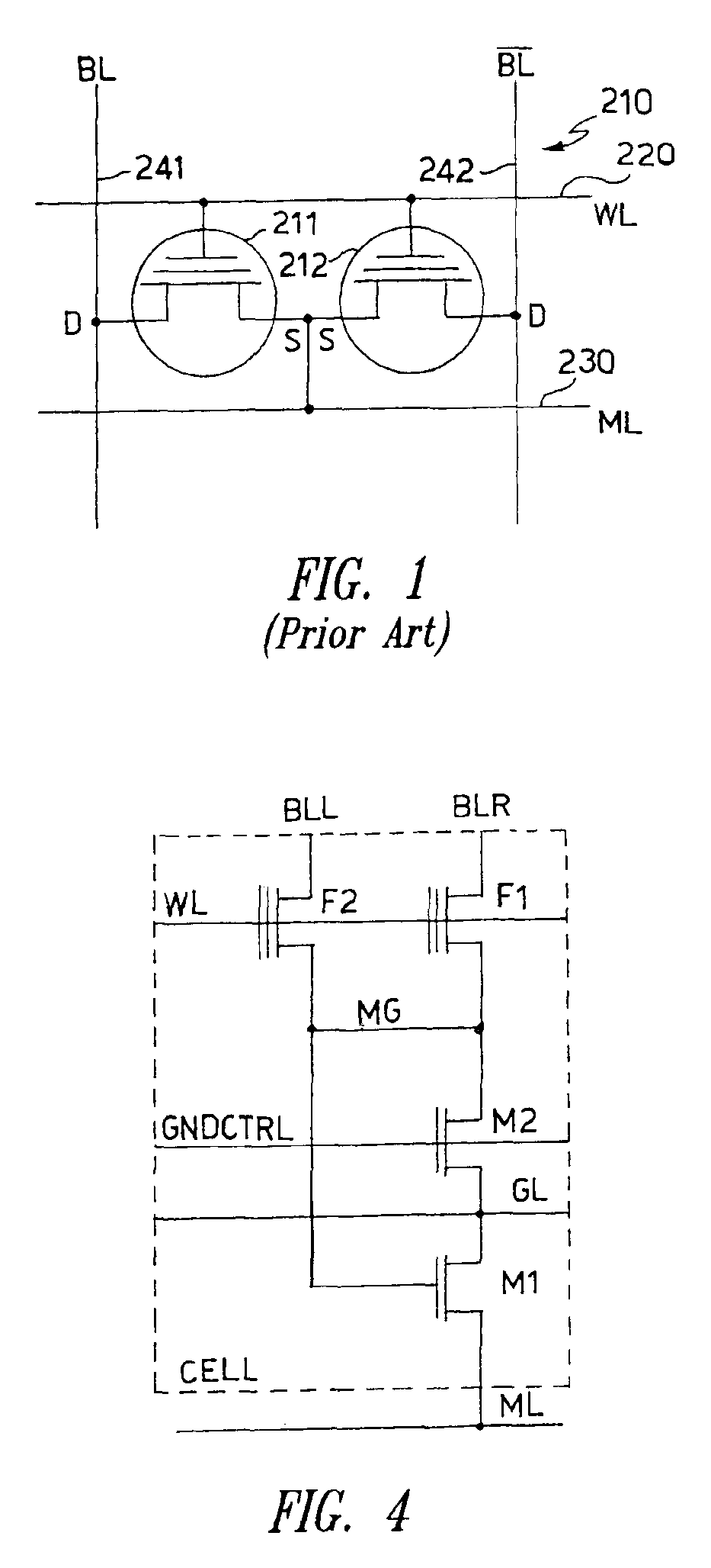
[0028]As can be seen from the circuit diagram of FIG. 4, each cell comprises four transistors: two floating-gate type transistors F1 and F2 with function of non-volatile memory ele...


PUM


Abstract

A non-volatile CAM-type memory having a multiplicity of memory cells ordered into a matrix of rows and columns, a word line and a match line associated with every row of cells and a first and a second bit line associated with every column of cells. In order to speed up the search for a data item in the memory and to simplify the circuit structure of the memory, each row of cells is associated with a ground control line and a ground line and every cell also includes a first controlled electronic switch connected between a ground line and a match line associated with the row containing the cell and having a control terminal connected to a match node of the cell and a second controlled electronic switch connected between the match node of the cell and the ground line associated with the row containing the cell, and further having a control terminal connected to the ground control line associated with the row containing the cell.

Description

BACKGROUND OF THE INVENTION[0001]1. Field of the Invention[0002]The present invention relates to semiconductor memories and, more particularly, a non-volatile memory of the CAM type, i.e., capable of being addressed by means of its content.[0003]2. Description of the Related Art[0004]As is known, semiconductor memories, such as used in microprocessors, computers, and the like, consist of a large number of cells arranged in rows and columns to form a cell matrix. Each cell contains a binary information element (bit) and to each row of the matrix there corresponds a binary word whose length depends on the number of columns.[0005]At present the most widely used memories are the static and dynamic RAMs (Random Access Memories) in which the word memorized in a row of the matrix can be accessed by simply furnishing its address. In the case of a CAM cell matrix, on the other hand, a binary word stored in a row can be looked for by inserting the word to be found in a comparison register ass...

Claims


Application Information

Patent Timeline
Patent Type & Authority Patents(United States)
IPC IPC(8): G11C15/00G11C15/04
CPCG11C15/046
Inventor DE SANDRE, GUIDO
Owner STMICROELECTRONICS SRL
Why Eureka
Try Eureka