Spot grid array electron imaging system

Inactive Publication Date: 2005-09-20
APPLIED MATERIALS INC
View PDF43 Cites 8 Cited by
  • Summary
  • Abstract
  • Description
  • Claims
  • Application Information

AI Technical Summary

Benefits of technology

[0011]The present invention provides an electron beam spot grid array imaging system instead of an optical imagin

Problems solved by technology

Disadvantageously, when conducting high-resolution inspection of large semiconductor substrates, the FOV of the imaging system cannot cover the entire substrate to be inspected, so the substrate must be moved or “stepped” across the FOV, thereby increasing inspection time.
These and other previous implementations of spot-grid array concepts suffer from several limitations.
However, some major problems prevent the use of prior art technologies for large arrays, such as relatively limited focus capabilities, imaging linearity, dielectric layer interference, and limited fault detection and classification capabilities.
One limitation of prior art optical spot grid array implementations arises from the fact that inspecting with confocal imaging requires very tight focus control, which is very difficult to achieve at high scan rates with large numerical aperture short-wavelength optics.
However, while taking several height-slice images sequentially, as described in the prior art, is compatible with a one frame review mode, it is not compatible with the continuous motion requirements of inspection systems.
Another limitation to large arrays in the prior art is the linearity requirem

Method used


Image

  • Spot grid array electron imaging system
  • Spot grid array electron imaging system
  • Spot grid array electron imaging system

Examples


example 1

[0051]FOV=1 mm=1000 micron[0052]DR=10 Giga-pix / sec=1010 pix / sec[0053]P=100 nm=0.1 micron[0054]→N=1000 / 0.1=10,000=104=>a 100 by 100 array;[0055]→FR=1010 / 104=106=1 mega-frames / second[0056]→V=106*0.1 micron=100 mm / sec

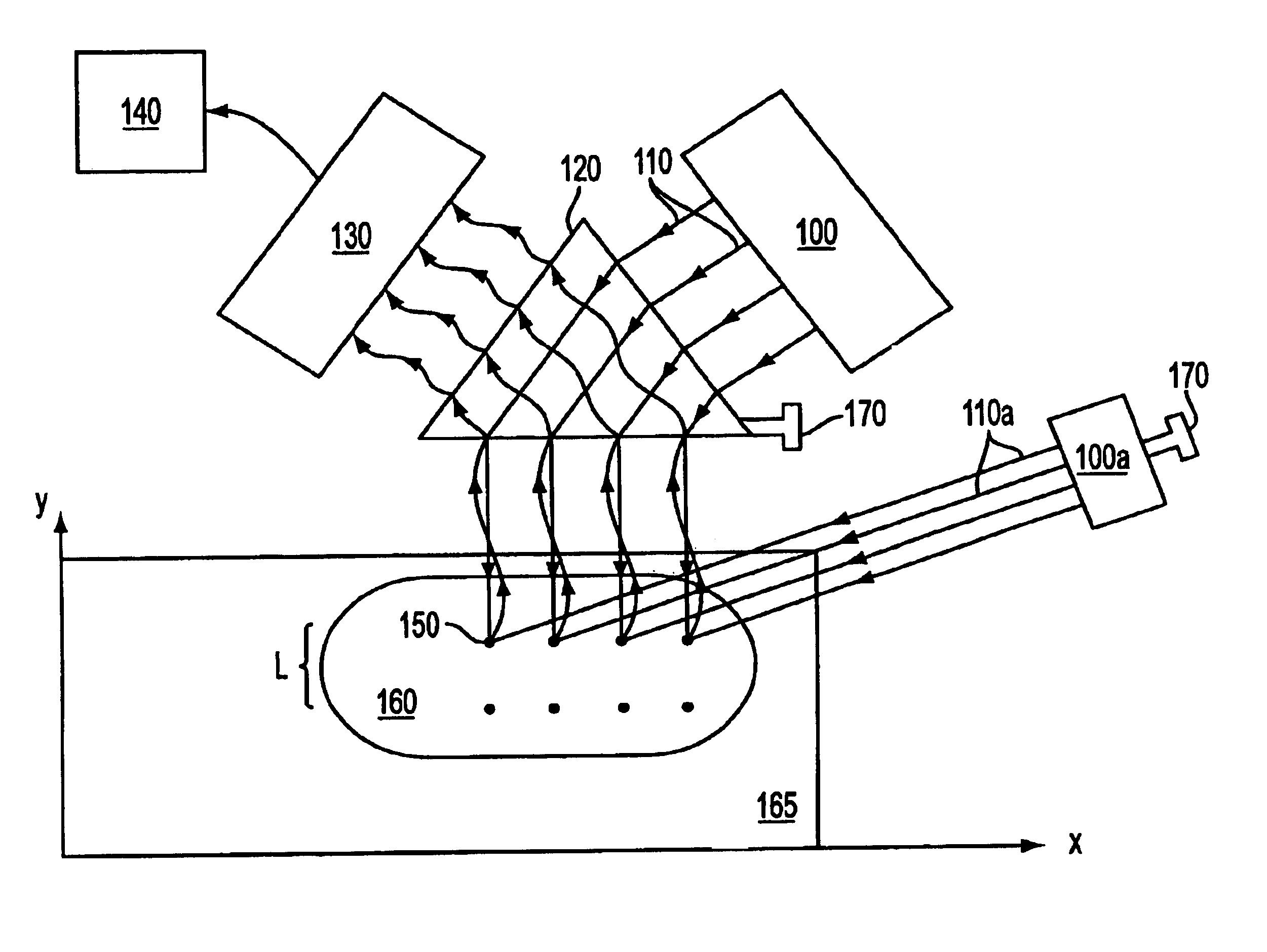
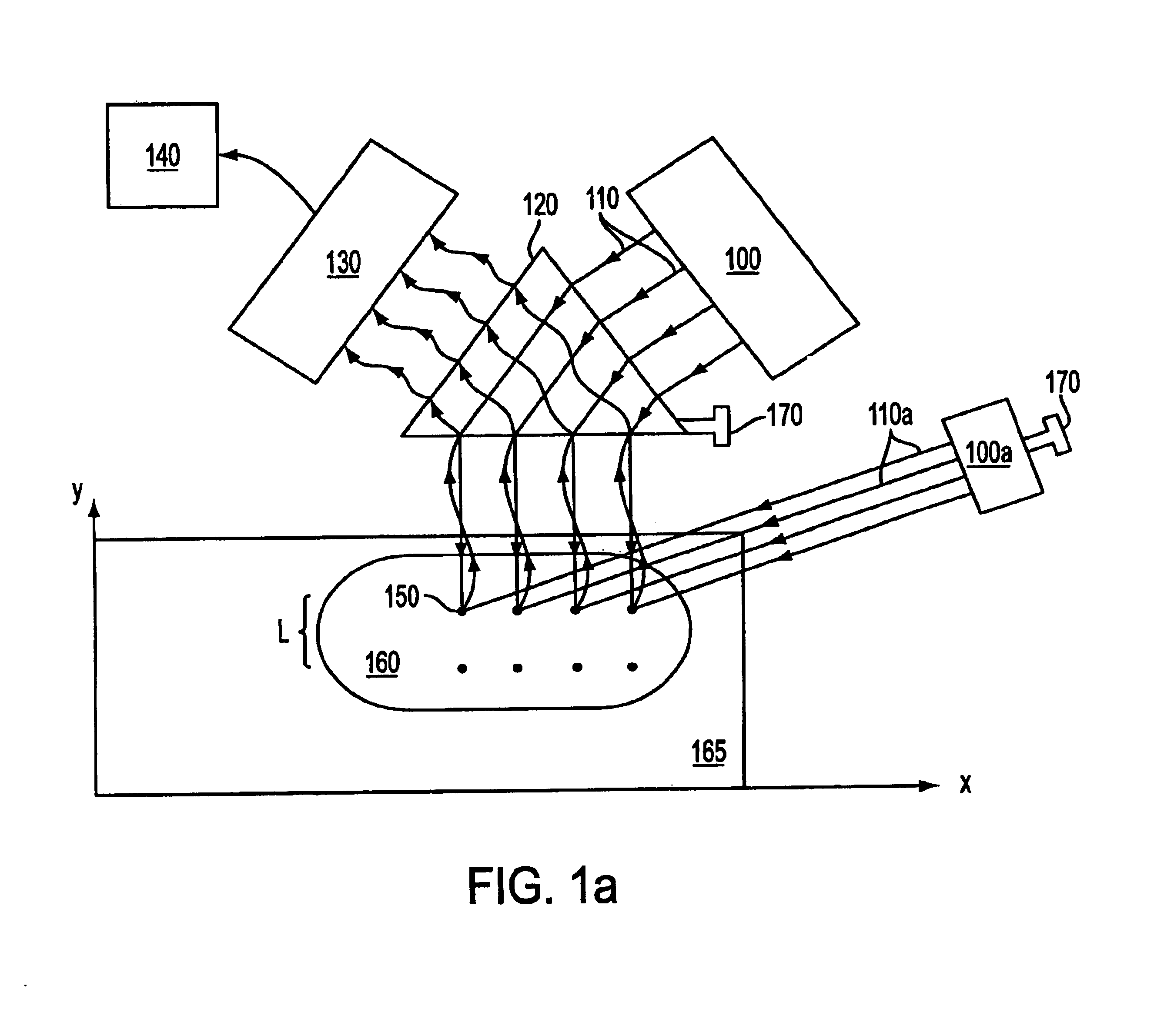
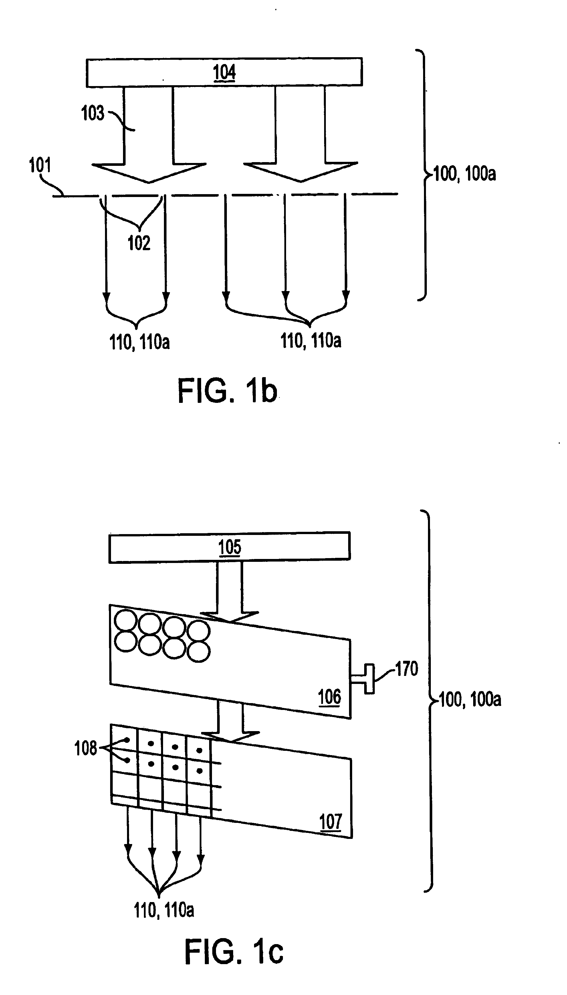
[0057]For a given pixel size, increasing the FOV is key to obtaining a larger number of pixels in the array, and hence to reduced frame-rates and stage velocity requirements (when using interleaving as shown in FIG. 3b, the number of rows and hence array elements increases and the frame-rate goes down, but the stage velocity requirement remains unchanged). This is an issue when using electron beam imaging and an electron-imaging column to focus multiple electron beams.

example 2

[0058]If the pixel size is reduced to 10 nm and the FOV is increased to 10 mm, the total number of array spots is N=10,000 / 0.01=106. Keeping the frame-rate (FR) at 106 frames / second, the data rate (DR) of the present invention becomes 1012 pixels / second or one Tera-pixels / second. The stage velocity (V) at this DR is 10 mm / sec. This system according to the present invention is three orders of magnitude faster than any prior art system. Of course, such a system requires conventional image acquisition and image processing systems capable of handling a high data-rate.


PUM


Abstract

A high data-rate electron beam spot-grid array imaging system is provided that overcomes the low resolution and severe linearity requirements of prior art systems. Embodiments include an imaging system comprising an electron beam generator for simultaneously irradiating an array of spots spaced apart from each other on a surface of an object to be imaged, and a detector for collecting backscattered and/or secondary electrons emitted as a result of the interaction of the spots with the surface of the object to form an image of the irradiated portions of the object surface. A mechanical system moves the substrate in a direction which is nearly parallel to an axis of the array of spots such that as the substrate is moved across the spot array in the scan direction (the y-direction) the spots trace a path which leaves no gaps in the mechanical cross-scan direction (the x-direction). A compensator, such as a servo or a movable mirror, compensates for mechanical inaccuracies in the moving stage, thereby increasing imaging accuracy. In other embodiments, multiple detectors placed at different angles to the substrate collect electrons to provide multiple perspective imaging of the substrate surface.

Description

RELATED APPLICATIONS[0001]The present application is related to Applicants' application Ser. No. 09 / 986,138, entitled SPOT GRID ARRAY IMAGING SYSTEM, filed Nov. 7, 2001, entitled SPOT GRID ARRAY IMAGING SYSTEM, which matured into U.S. Pat. No. 6,639,201, issued Oct. 28, 2003.FIELD OF THE INVENTION[0002]The present invention relates to an electron beam imaging system. The present invention has particular applicability in imaging systems optimized for automated defect inspection.BACKGROUND ART[0003]Automated inspection is a technique for measuring the integrity of an object by collecting an image of it and comparing that image to a reference (e.g., comparing a die to a data-base for photolithographic masks), to another part of that object (such as die-to-die inspection for semiconductor wafers), or to a reference image (die-to-“golden image”). Disadvantageously, when conducting high-resolution inspection of large semiconductor substrates, the FOV of the imaging system cannot cover the...

Claims


Application Information

Patent Timeline
IPC IPC(8): H01J37/28G01Q10/00G01Q30/02G01Q30/06
CPCH01J37/28H01J2237/024H01J2237/0635H01J2237/1503H01J2237/20228H01J2237/2817H01J37/20H01J37/244
Inventor ALMOGY, GILADRECHES, OREN
Owner APPLIED MATERIALS INC
Why Eureka
Try Eureka