Level transforming circuit

a level-transforming circuit and level-transforming technology, applied in logic circuit coupling/interface arrangement, pulse generator, pulse technique, etc., can solve the problems of complex manufacturing process, not operating rapidly, and level-transforming circuit of the conventional art. achieve fast output circuit, pass current, and operation can be fast

Inactive Publication Date: 2005-09-20
LAPIS SEMICON CO LTD
View PDF6 Cites 20 Cited by
  • Summary
  • Abstract
  • Description
  • Claims
  • Application Information

AI Technical Summary

Benefits of technology

[0037]According to the above configuration, electric potential exceeding the low voltage level is not statically impressed with the gate oxide film of each transistor. Therefore, a level transforming circuit is able to comprise only MOS transistors whose endurable strength of gate oxide film is lower than the high voltage electricity source level. In addition, the latch circuit comprises a CMOS invertor. On the other hand, the second prior art mentioned above (FIG. 2) employs an effect of turning off of the source follower transistor in order to limit amplitude of gate voltage. Therefore, the first aspect of present invention is able to operate faster than the second prior art and to restrain a drivability drop. Especially, as for an SOI device of a depletion type, whose dielectric strength between source and drain is low owing to its structure; the first aspect of present invention is extremely useful, because overvoltage is not impressed between the source and drain.
[0066]Moreover, a first signal is a signal having an amplitude between the high voltage and the low voltage, and the first signal is output independently of the output signal. According to the above structure, operation can be fast and drop of load drivability can be restrained. Moreover, a range of adaptation of a level transforming circuit becomes wide.

Problems solved by technology

However, the level transforming circuit of the conventional art have problems.
Thus, there is a problem that a manufacturing process becomes complicated.
The level transforming circuit of the second prior art uses this motion, and therefore, could not operate rapidly.
Therefore, there is another problem that the ability to bear a load of the output section decreases.
Thus, an ability of the device is deteriorated by a hot carrier.
As a result, a problem was caused in that the reliability of the device deteriorates.
Thus, the ability of the device is deteriorated by a hot carrier.
As a result, a problem was caused in that the reliability of the device deteriorates.
As a result, a problem is caused of increasing electricity consumption in vain.
As a result, a problem is caused of deteriorating high mobility of the output stage.

Method used


Image

  • Level transforming circuit
  • Level transforming circuit
  • Level transforming circuit

Examples


embodiment 1

Effect of Embodiment 1

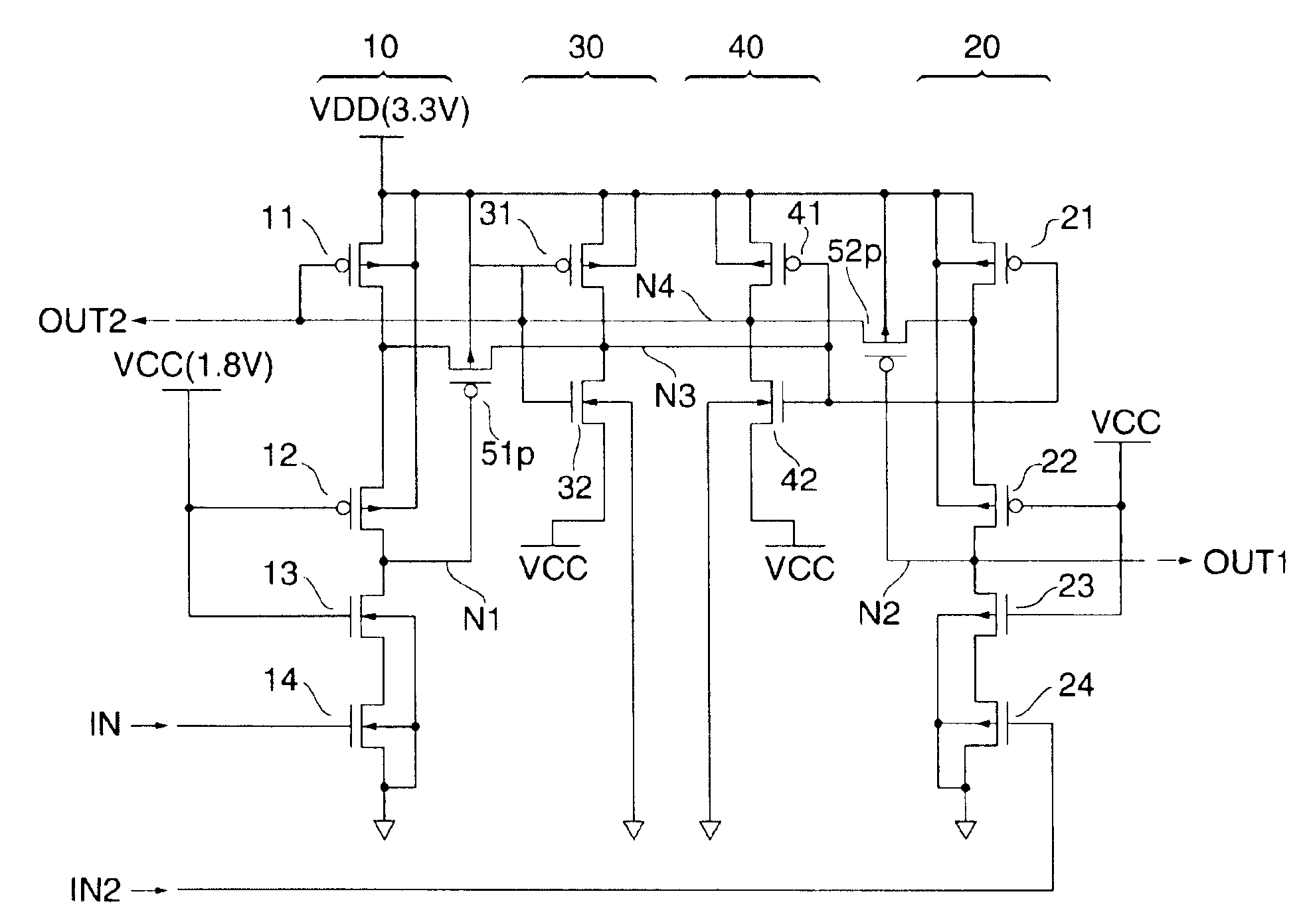
[0108]As mentioned above, according to Embodiment 1, the gate oxide film of each transistor mentioned above is not impressed with an electric potential exceeding the low voltage level statically. Therefore, a level transforming circuit can comprise a MOS transistor where an acceptable dielectric strength of the gate insulating film is lower than the high voltage level. The latch circuit comprises a CMOS inverter. Thus, the voltage between the gate and the source impressed with each transistor of the CMOS inverter transiently becomes lower than the low voltage level. Thus, the level transforming circuit of present invention operates faster than the second conventional art (FIG. 11), and a drop of load bearing ability can be restrained.

[0109]Moreover, according to Embodiment 1, the level transforming circuit comprises the intermediate circuit consisting of the MOS transistor and the CMOS inverter. Thus, the voltage between the gate and the source impressed with e...

embodiment 2

Effect of Embodiment 2

[0118]As described above, according to Embodiment 2, voltage exceeding the strength between the source and the drain is never impressed between the source and the drain of each transistor mentioned above, even in a transient state. Therefore, the level transforming circuit can comprise only a MOS transistor whose source-drain strength is lower than the high voltage electricity source. Moreover, a voltage exceeding the low voltage level is never impressed with the gate oxide film of each transistor mentioned above, even in transient state. Therefore, a reliable level transforming circuit can comprise only the MOS transistor whose strength of gate oxide film is lower than the high voltage electricity source level.

Embodiment 3

[0119]FIG. 3 shows a level transforming circuit according to Embodiment 3. In FIG. 3, elements that are the same as Embodiment 1 are designated with the same symbols.

[0120]Embodiment 3 is different from Embodiment 1 or 2 in the following poin...

embodiment 3

Effect of Embodiment 3

[0122]In Embodiment 3, NMOS 32 and 42 are formed in a P well region electrically separated from the semiconductor substrate, and PMOS 51p and 52p are separated from the N well of other PMOS. Substrates of NMOS 32, 42 and PMOS 51p, 52p are connected with their own sources respectively. Therefore, an effect is obtained of further relieving load to the gate oxide film of NMOS 32, 42 and PMOS 51p, 52p. Moreover, inverse bias voltage impressed with the pn junction is relieved, which is formed by the drain and the substrate of NMOS 32 and 42. Moreover, faster operation of the circuit is expected because influence of substrate bias on the operation of circuit does not exist about NMOS 32 and 42.

[0123]An element isolation technique such as triple well structure applied to Embodiment 3 has been adopted for LSI made by a fine process for the purpose of reducing substrate noise or reducing leak current, and the cost of production increases by several percent. But, this te...


PUM


Abstract

A level trasnforming circuit includes a first CMOS circuit, a first intermediate circuit, a second intermediate circuit, a second CMOS circuit, a seventh p-channel type MOS transistor, and an eighth p-channel type MOS transistor; wherein the first intermediate circuit and the second intermediate circuit form a latch circuit. To this latch circuit, writing of data is performed by way of the seventh p-channel type MOS transistor and the eighth p-channel type MOS transistor. Thus, the latch circuit is made up of a CMOS inverter. Therefore, fast operation can be obtained and drop of drivability can be restrained.

Description

BACKGROUND OF THE INVENTION[0001]1. Field of the Invention[0002]The present invention relates to a level transforming circuit serving as an interface of a digital circuit, wherein the level transforming circuit operates with different electricity source voltages.[0003]2. Description of Related Art[0004]The finer the structure of a MOS transistor becomes, the weaker the strength of a gate oxide film becomes. For example, a MOS transistor produced in a fine process of an extent of 0.35 μm is able to operate at an electricity source voltage of an extent of 3.3V. Further, a MOS transistor produced in a latest fine process of an extent of 0.18 μm is able to operate at an electricity source voltage of an extent of 1.8V. In the conventional art, when it is necessary to make an interface between a circuit of 0.18 μm fine process and a circuit of 0.35 μm fine process, a level transforming circuit in the interface required both MOS transistors of 1.8V and 3.3V.[0005](First Prior Art)[0006]FIG...

Claims


Application Information

Patent Timeline
Patent Type & Authority Patents(United States)
IPC IPC(8): H03K3/356H03K3/00H03K3/012H03K19/003H03K17/10H03K17/687H03K19/0185
CPCH03K3/356113H03K3/012
Inventor MITARASHI, MUTSUMI
Owner LAPIS SEMICON CO LTD
Why Eureka
Try Eureka