

Organic thin-film switching memory device and memory device
a memory device and thin film technology, applied in solid-state devices, instruments, nanoinformatics, etc., can solve the problems of difficult implementation of large-capacity organic memory devices and memory devices, high-performance organic memory devices or memory devices
- Summary
- Abstract
- Description
- Claims
- Application Information
AI Technical Summary
Benefits of technology
Problems solved by technology
Method used
Image

Examples
first embodiment
[0021
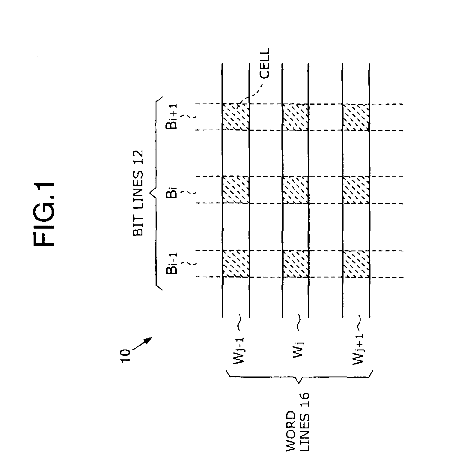
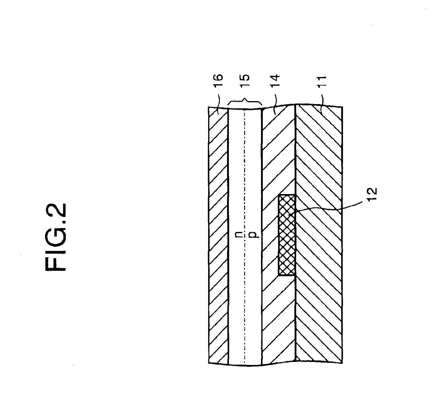
[0022]FIG. 1 is a plan view of part of a memory device 10 according to a first embodiment of the present invention, and FIG. 2 is a cross-sectional view of a region that comprises a memory cell portion of the memory device 10 shown in FIG. 1. As shown in FIG. 1, the memory device 10 is constituted by stacking, on a substrate 11, a lower electrode (hereinafter, also referred to as bit lines Bi) 12, a memory layer 14, a semiconductor layer 15, and an upper electrode (hereinafter, also referred to as word lines Wj) 16, in this order.
[0023]In more detail, the substrate 11 is constituted by alkali-free glass, for example. A plurality of first electrode lines made of a gold (Au) metal layer or other metal layer, that is, bit lines Bi (i=1, 2, . . . m), are arranged in the form of mutually parallel stripes or strips on the substrate 11. The memory layer 14 is formed by an organic memory material such as zinc phthalocyanine (ZnPc) or zinc phthalocyanine porphyrin, for example. The semi...
second embodiment
[0039
[0040]FIG. 10 is a cross-sectional view of a region which includes a memory cell portion of the memory device 10 according to a second embodiment of the present invention. The semiconductor layer 15 is formed as a p-type organic semiconductor for which the material used is copper phthalocyanine. A Schottky diode junction is formed at the interface with the semiconductor layer 15 by using a metal having a work function that is smaller than that of copper phthalocyanine, such as aluminum (Al), for example, for the upper electrode (word line Wj) 16. The configuration of the other portions of the memory device 10 is similar as that of the first embodiment.
[0041]Similarly to the case of the first embodiment described above, the Schottky diode exhibits a favorable switching characteristic and the cells C(j+1,i) thus operate as switching memory cells.
third embodiment
[0042
[0043]FIG. 11 is a cross-sectional view of a region which includes a memory cell portion of the memory device 10 according to a third embodiment of the present invention. In this embodiment, the configuration is produced by changing the position of the memory layer and the semiconductor layer of the first embodiment. More particularly, a bit line 12, a semiconductor layer 15, an organic memory layer 14, and a word line 16 are formed in this order on a substrate 11. Further, in this case, the semiconductor layer 15 is a p-n junction diode, for example, and is constituted such that the p-type semiconductor layer thereof makes contact with the lower electrode (bit line) 12. The configuration is in other respects similar to the first embodiment.
[0044]Further, a variety of additional modifications are possible for the above-described first to third embodiments. For example, a configuration is possible in which the word line and bit line are switched. More particularly, the lower ele...
PUM
 Abstract
Description
Claims
Application Information