CMOS image sensor integrated together with memory device

a memory device and image sensor technology, applied in the field of cmos (complementary metal oxide silicon) image sensors, can solve the problems of large power consumption, difficult to make a signal processing circuit integrated into a ccd chip, and many demerits of the ccd (charge coupled device) image sensor, so as to reduce the cost and power consumption and minimize the system

Inactive Publication Date: 2005-09-27
PHOTONIC IMAGING SOLUTIONS INC
View PDF12 Cites 16 Cited by
  • Summary
  • Abstract
  • Description
  • Claims
  • Application Information

AI Technical Summary

Benefits of technology

[0007]It is, therefore, an object of the present invention to provide a CMOS image sensor integrated together with a memor

Problems solved by technology

Generally, a CCD (charge coupled device) image sensor has many demerits in that complicated operation methods, large power consumption and a number of mask processes are required.
Furthermore, it is very difficult to make a signal processing circuit integrated into a CCD chip.
However, in the conventional image sensor, since me

Method used


Image

  • CMOS image sensor integrated together with memory device
  • CMOS image sensor integrated together with memory device
  • CMOS image sensor integrated together with memory device

Examples


Embodiment Construction

[0013]Hereafter, the present invention will be described in detail with reference to the accompanying drawings.

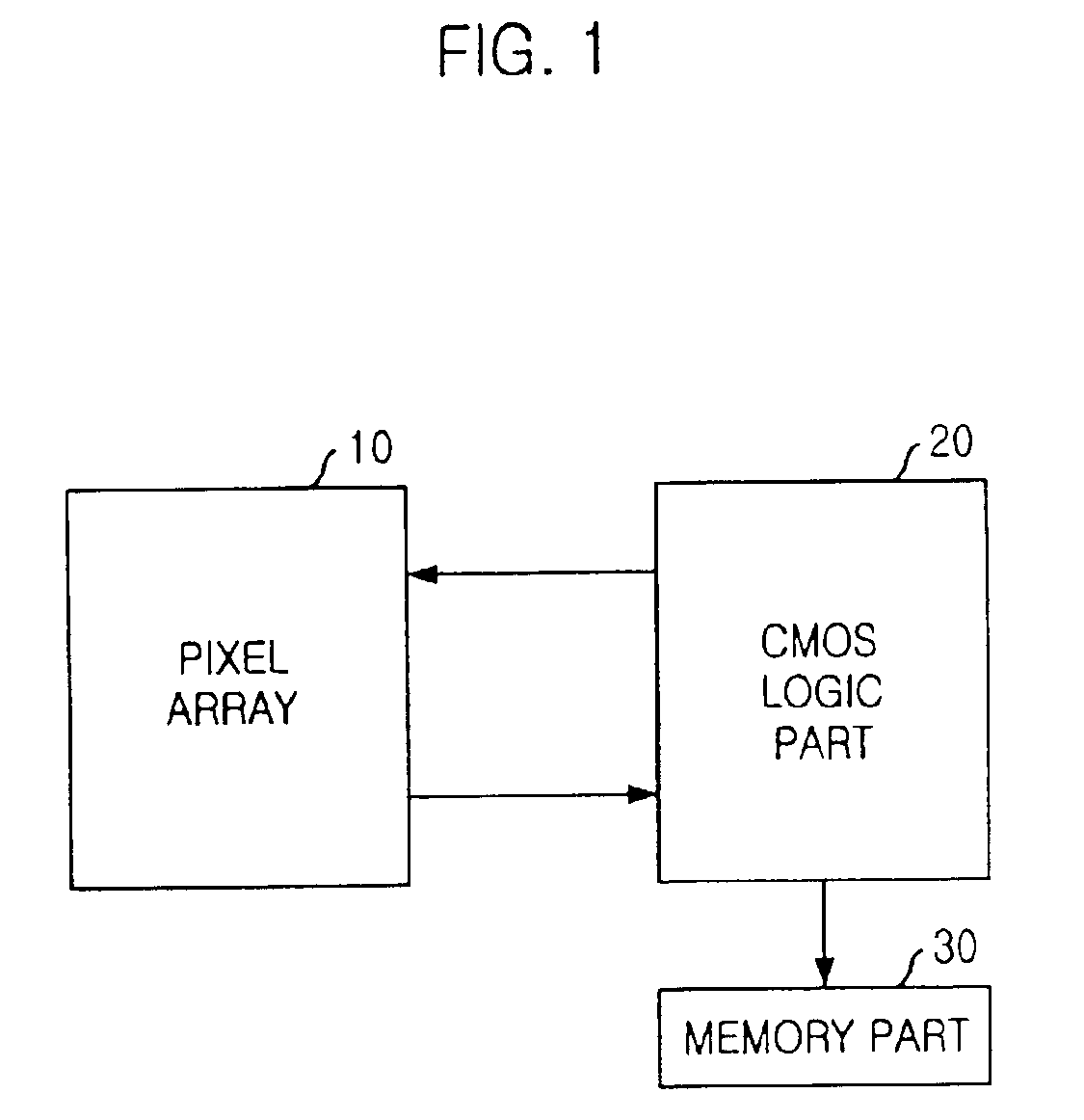
[0014]FIG. 1 is a schematic diagram illustrating a CMOS image sensor in accordance with the present invention. As illustrated in FIG. 1, a CMOS image sensor in accordance with the present invention includes a pixel array 10 where pixels having photodiodes are arrayed, a CMOS logic part 20 for controlling the pixel array 10 and processing output signal from the pixel array 10 and a memory part 30 for storing image data processed in the CMOS logic part 20. The pixel array 10, the CMOS logic part 20 and the memory part 30 are integrated into one chip. Also, the memory part 30 may be composed of DRAMs or SRAMs.

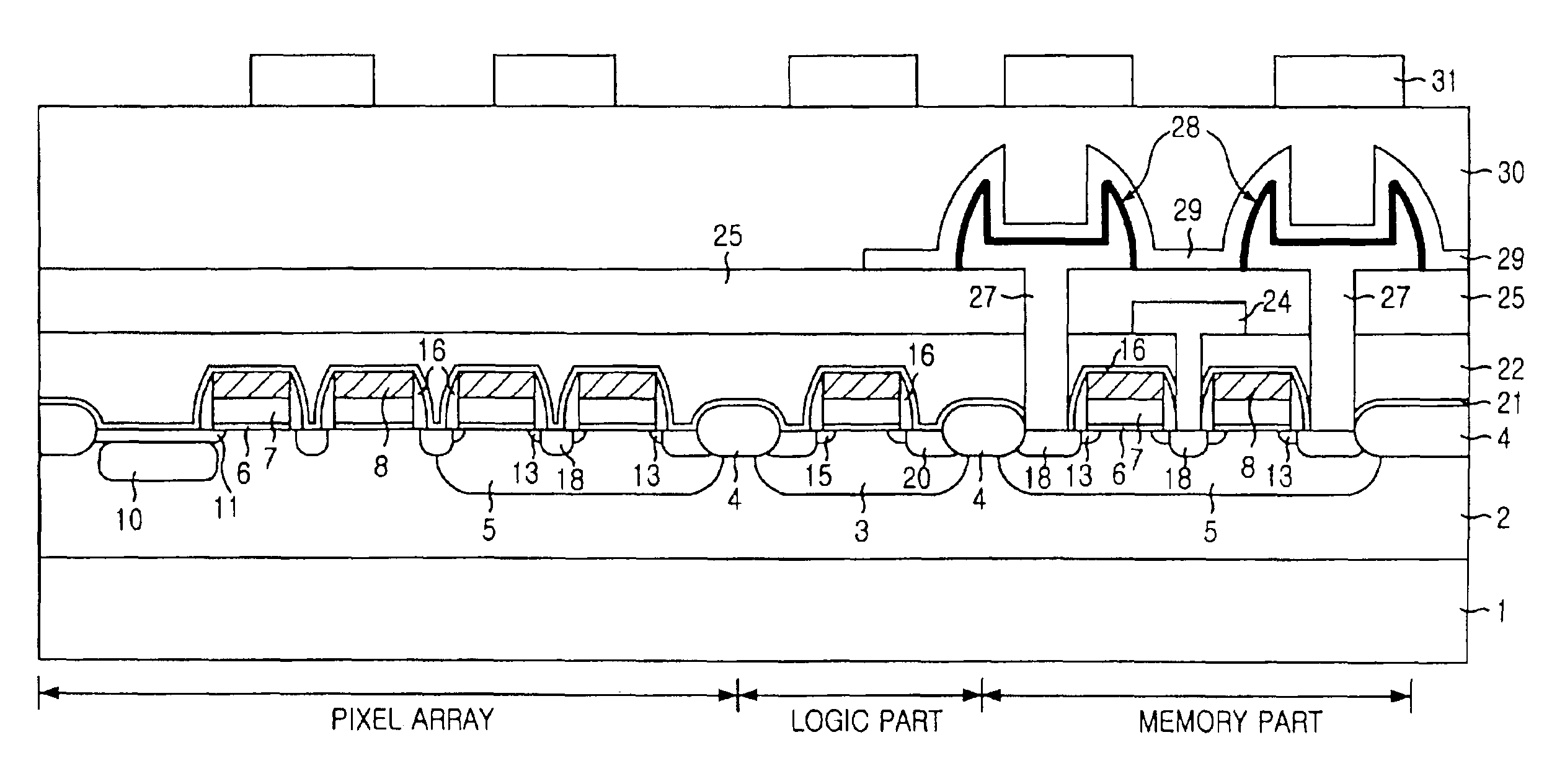
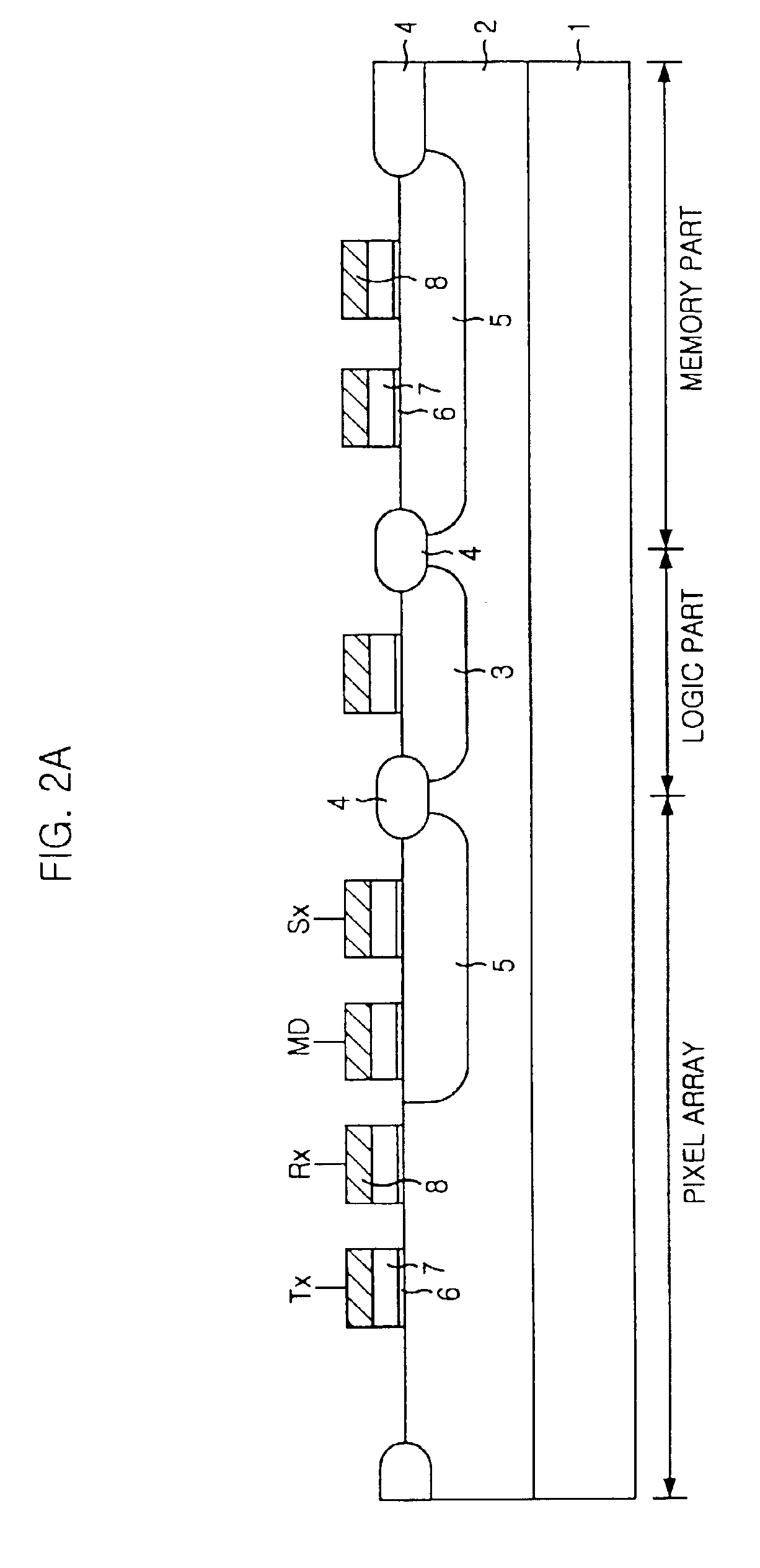
[0015]FIGS. 2A to 2J are cross-sectional views illustrating a chip on which a CMOS image sensor and a DRAM are integrated in accordance with the present invention. In order to simplify the explanation, a pixel array, a CMOS logic part and a memory part are respectively sh...


PUM


Abstract

The present invention relates to a CMOS (Complementary Metal Oxide Silicon) image sensor; and, more particularly, to an image sensor integrated into one chip, together with a memory. The CMOS image sensor according to the present invention comprises: a pixel array formed on a chip, having a plurality of unit pixels; a logic circuit formed on the chip to process signals form the pixel array; and a memory formed on the chip to store outputs from the logic circuit, wherein the pixel array, the logic circuit and the memory are isolated from each other by insulating layers, whereby the pixel array, the logic circuit and the memory are integrated on the same chip.

Description

[0001]This patent application is a division of U.S. patent application Ser. No. 09 / 342,343, filed Jun. 29, 1999 now 6,563,184, incorporated herein in its entirety.FIELD OF THE INVENTION[0002]The present invention relates to a CMOS (Complementary Metal Oxide Silicon) image sensor; and, more particularly, to an image sensor integrated into one chip, together with a memory.DESCRIPTION OF THE PRIOR ART[0003]Generally, a CCD (charge coupled device) image sensor has many demerits in that complicated operation methods, large power consumption and a number of mask processes are required. Furthermore, it is very difficult to make a signal processing circuit integrated into a CCD chip. Accordingly, in order to overcome such demerits, many developments for a CMOS image sensor have been recently unsued using a submicron CMOS manufacturing technique. A CMOS image sensor creates a picture by detecting signals from photodiodes and MOS transistors formed within a unit pixel. The use of a CMOS manuf...

Claims


Application Information

Patent Timeline
IPC IPC(8): G11C13/04H01L27/10H01L21/8242H01L27/108H01L27/146
CPCG11C13/04H01L27/14634H01L27/14643H01L27/10814H01L27/10873H01L27/10894H01L27/14609H10B12/315H10B12/05H10B12/09H01L27/10
Inventor PARK, SANG HOON
Owner PHOTONIC IMAGING SOLUTIONS INC
Why Eureka
Try Eureka