Liquid crystal display and method of manufacturing the same

a technology of liquid crystal display and pad terminal, which is applied in the direction of basic electric elements, electrical equipment, semiconductor devices, etc., can solve the problems of image quality degradation of lcd screen, and achieve the effect of improving the quality of displayed images

Inactive Publication Date: 2005-09-27
LG DISPLAY CO LTD
View PDF9 Cites 7 Cited by
  • Summary
  • Abstract
  • Description
  • Claims
  • Application Information

AI Technical Summary

Benefits of technology

[0019]One object of the present invention is to keep contact resistance of a pad terminal surface of an active panel at a low level.
[0020]Another object of the present invention is to maintain the scan and data signals in their original state by keeping contact resistance of the pad terminal at a low level.
[0021]Yet another object of the present invention is to enhance the quality of a displayed image by maintaining the signals of the active panel in their original state.

Problems solved by technology

If there are particles or contaminants between the pad terminal and the output terminal of the outer device, or if the electrical contact between them is poor, then the quality of the image on the LCD screen may degrade.

Method used


Image

  • Liquid crystal display and method of manufacturing the same
  • Liquid crystal display and method of manufacturing the same
  • Liquid crystal display and method of manufacturing the same

Examples


Embodiment Construction

[0037]Reference will now be made in detail to the preferred embodiments of the present invention, examples of which are illustrated in the accompanying drawings.

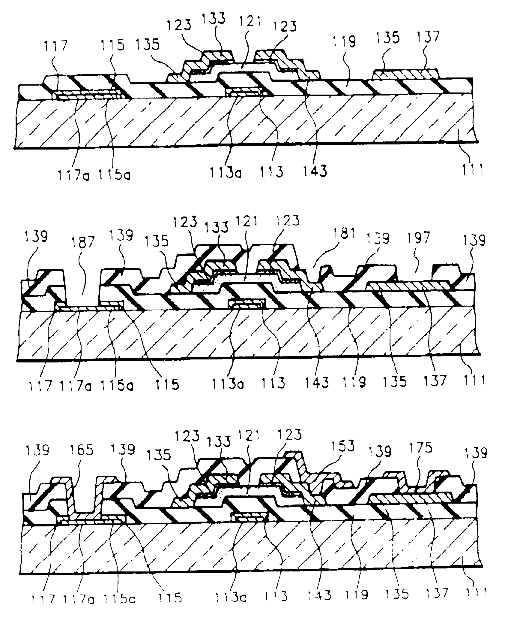
[0038]The present invention relates to a method for maintaining contact resistance of a pad and the structure of the pad. The present invention prevents contamination by foreign materials, such as an oxidation layer or a nitrification layer, of the pad surface during the manufacture of an LCD active panel Thus, contact resistance does not increase due to the contaminating materials. Also, the pad surface may have a raised part and a depressed part, enlarging the total contact area of the pad. Therefore, contact resistance and adhesion between the pad and the pad terminal are improved. Thus, a high quality LCD panel can be manufactured.

[0039]The present invention therefore discloses a manufacturing method of an active panel where the pad terminal surface does not have a thin layer of particles which increase contact resistanc...


PUM


Abstract

In manufacturing an active panel of a liquid crystal display, when a pad portion to which outer driving signals are applied is formed, oxide or nitride layer is generated on the surface of the pads. Since these oxide and nitride layers have a high intrinsic resistance, they cause a reliability of the signal transmission in the pad portion to be decreased. The present invention provides a method for enhancing the reliability of the signal transmission in the pad portion by removing contaminants such as oxide layer and nitride layer and reducing the contact resistance of the pad portion. The present inversion also provides a method for maintaining a good adhesion by forming a surface of the pad portion in an uneven shape and by increasing the contact area. The pad is formed from dual metal layer made by depositing sequentially a first metal layer and a second metal layer. A protection layer is formed by depositing an insulation material such a silicon oxide or silicon nitride on the entire surface of the substrate on which the pad is formed. By etching the protection layer using dry etching method, a pad contact hole is formed on the pad. The second metal of the pad is removed by wet etching method, using the pad contact hole as mask. By doing so, the contaminants between the metal layer and the protection layer can be completely removed. Further, the present invention can have a plurality of pad contact holes to enlarge the contact area between the pad and the pad terminal, and thereby enhancing adhesion between the pad and the pad terminal.

Description

[0001]This application is a divisional of U.S. application Ser. No. 08 / 993,195, filed Dec. 18, 1997, now U.S. Pat. No. 6,288,414 the entire disclosure of which is considered to be part of the disclosure of the accompanying application and is hereby incorporated by reference therein.[0002]This application claims the benefit of Korean patent application No. P97-7226, filed Mar. 5, 1997, which is hereby incorporated by reference.BACKGROUND OF THE INVENTION[0003]1. Field of the Invention[0004]The present invention relates to a method for manufacturing a pad terminal for inputting or outputting electrical signals. More particularly, the present invention relates to a structure of the pad terminal to an electrical circuit board or a liquid crystal display device, and a method of manufacturing of the pad terminal.[0005]2. Description of the Background Art[0006]Generally, most electrical circuit boards have pad terminals for inputting or outputting electrical signals. These pad terminals ar...

Claims


Application Information

Patent Timeline
Patent Type & Authority Patents(United States)
IPC IPC(8): H01L21/00H01L21/77H01L27/12
CPCH01L27/14621H01L27/14687H01L27/124
Inventor AHN, BYUNG CHOL
Owner LG DISPLAY CO LTD
Why Eureka
Try Eureka