Method for fabricating capacitor of semiconductor device

Inactive Publication Date: 2005-09-27
SK HYNIX INC
View PDF4 Cites 5 Cited by
  • Summary
  • Abstract
  • Description
  • Claims
  • Application Information

AI Technical Summary

Benefits of technology

[0022]Accordingly, the present invention has been made to solve the above-mentioned problems occurring in the prior art, and an object of the present invention is to provide a method for fabricating a capacitor of a semiconductor device, which can fundamentally pro

Problems solved by technology

According to the advance of high integration of the semiconductor device, capacitors fabricated in a cylinder shape by the conventional process have a limitation of capacitance security.
However, wi

Method used


Image

  • Method for fabricating capacitor of semiconductor device
  • Method for fabricating capacitor of semiconductor device
  • Method for fabricating capacitor of semiconductor device

Examples


Example

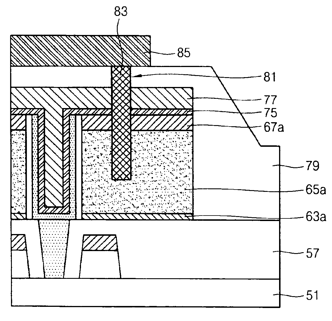
[0029]Hereinafter, preferred embodiments of the present invention will be described with reference to the accompanying drawings. In the following description and drawings, the same reference numerals are used to designate the same or similar components, and so repetition of the description on the same or similar components will be omitted.

[0030]FIGS. 2A to 2H are cross-sectional views showing each process of a method for fabricating a capacitor of a semiconductor device according to an embodiment of the present invention.

[0031]With a method for fabricating a capacitor of a semiconductor device according to a preferred embodiment of the present invention, as shown in FIG. 2A, bit lines 53 and a hard-mask layer 55 are formed on a semiconductor substrate 51 having a device isolation film and word lines, and then an interlayer insulating film 57 is deposited on the upper surface of the resultant lamination obtained through the above process.

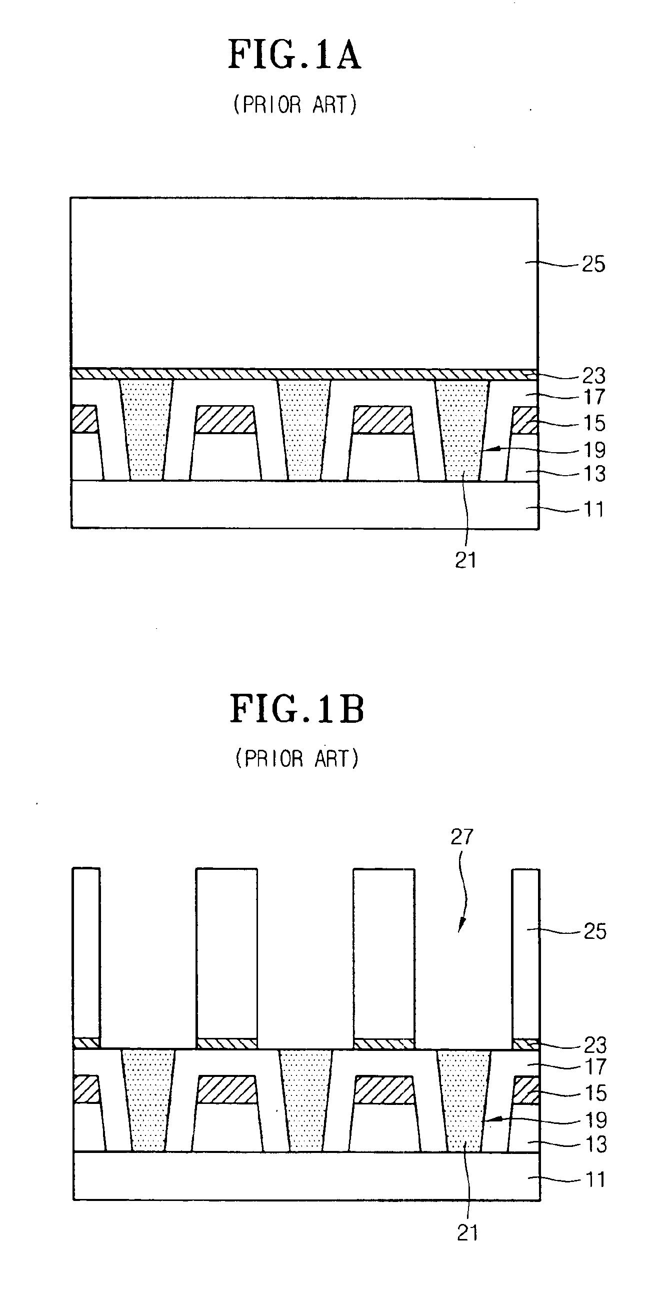
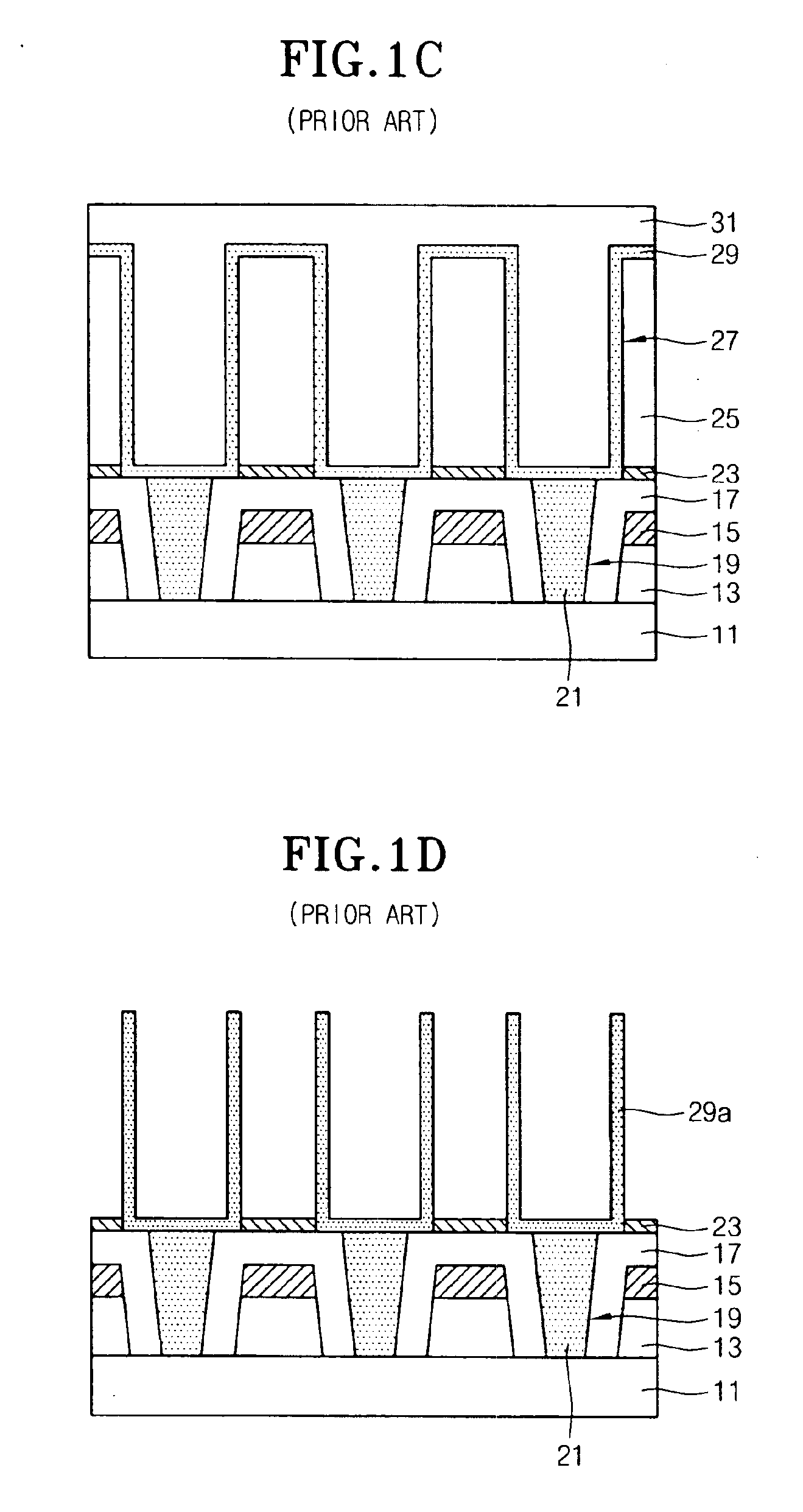
[0032]Then, after portions of the interlayer i...


PUM


Abstract

In fabricating a capacitor of a semiconductor device, a first contact plug is formed in a plug contact hole formed by patterning a portion of a first interlayer insulating film formed on a substrate. A first barrier layer, a first polysilicon layer, and a second barrier layer are formed. A first contact hole is formed after sequentially patterning the second barrier layer, the first polysilicon layer, and the first barrier layer. A first dielectric layer is formed to have portions located at outside and bottom parts of the first contact hole. A second polysilicon layer is formed to have its portions located at portions except for the first contact hole. A second dielectric layer and a third polysilicon layer are formed. A second interlayer insulating film is formed after patterning the third polysilicon layer. The second interlayer insulating film, the patterned third polysilicon layer, the second dielectric layer, the second barrier layer, and the first polysilicon layer are selectively removed to form a second contact hole and a second contact plug, and then forming a metal wiring.

Description

BACKGROUND OF THE INVENTION[0001]1. Field of the Invention[0002]The present invention relates to a method for fabricating a capacitor of a semiconductor device, and more particularly to a method for fabricating a capacitor which can secure a capacitance suitable for a high-integrated semiconductor device and also can improve the safety of a pattern.[0003]2. Description of the Prior Art[0004]According to the advance of high integration of the semiconductor device, capacitors fabricated in a cylinder shape by the conventional process have a limitation of capacitance security.[0005]As a cell pitch is reduced, the sectional area of a capacitor is reduced, and thus the height of the capacitor must be increased more and more in order to compensate for the reduced sectional area.[0006]However, with the consideration of pattern formation, even the increase of the height has a limitation. Also, it has been difficult to prevent the inclination of a storage nodes when a cylinder shape is forme...

Claims


Application Information

Patent Timeline
IPC IPC(8): H01L21/02H01L21/8242
CPCH01L28/91H10B99/00
Inventor SEO, WON SUN
Owner SK HYNIX INC
Why Eureka
Try Eureka