Image-sensing apparatus

a technology of image sensor and image, applied in the field of image sensor, can solve the problems of narrow dynamic range, flat blackness in dim portions of obtained images, and narrow dynamic range, and achieve the effect of accurate compensation data acquisition

Inactive Publication Date: 2005-09-27
SONY SEMICON SOLUTIONS CORP
View PDF8 Cites 9 Cited by
  • Summary
  • Abstract
  • Description
  • Claims
  • Application Information

AI Technical Summary

Benefits of technology

[0011]An object of the present invention is to provide a solid-state image-sensing device that, without requiring irradiation of uniform light beforehand, permits accurate acquisition of compensation data to be used to correct the outputs from individual pixels during shooting of a subject.
[0012]Another object of the present invention is to provide a solid-state image-sensing device in which variations in sensitivity among pixels are minimized by making the initial states of the individual pixels substantially identical.
[0013]Still another object of the present invention is to provide a solid-state image-sensing device in which variations in sensitivity among pixels are minimized by keeping the potentials at the surfaces of gate portions of the individual pixels substantially identical.

Problems solved by technology

A CCD-type image-sensing device accumulates photoelectric charges in potential wells while transferring them, and has the disadvantage of a comparatively narrow dynamic range.
This, however, leads to a narrow dynamic range and thus demands accurate control of the amount of exposure.
Moreover, even if the amount of exposure is controlled accurately, the obtained image tends to suffer from flat blackness in dim portions thereof and saturation in bright portions thereof.
This solid-state image-sensing device offers a wide dynamic range, but tends to suffer from different threshold-value characteristics among the MOS transistors provided in the individual pixels and thus varying sensitivity from one pixel to another.
However, it is troublesome for a user to illuminate the pixels with an external light source, and moreover it is difficult to illuminate them sufficiently uniformly.
On the other hand, providing an image-sensing apparatus with a mechanism for illuminating uniform light complicates the structure of the image-sensing apparatus.

Method used


Image

  • Image-sensing apparatus
  • Image-sensing apparatus
  • Image-sensing apparatus

Examples


first embodiment

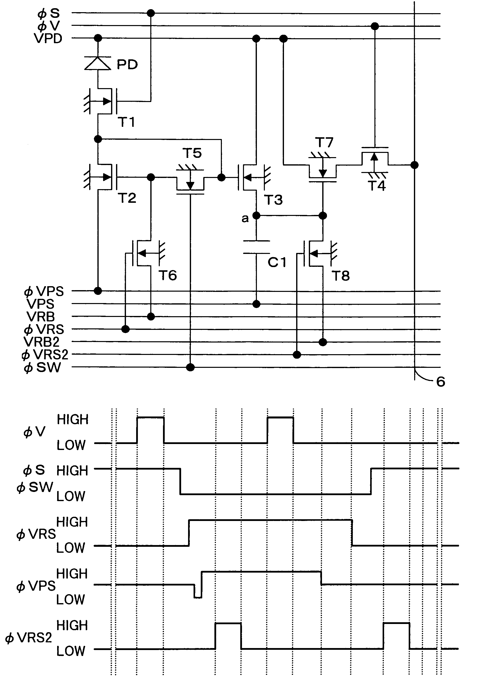
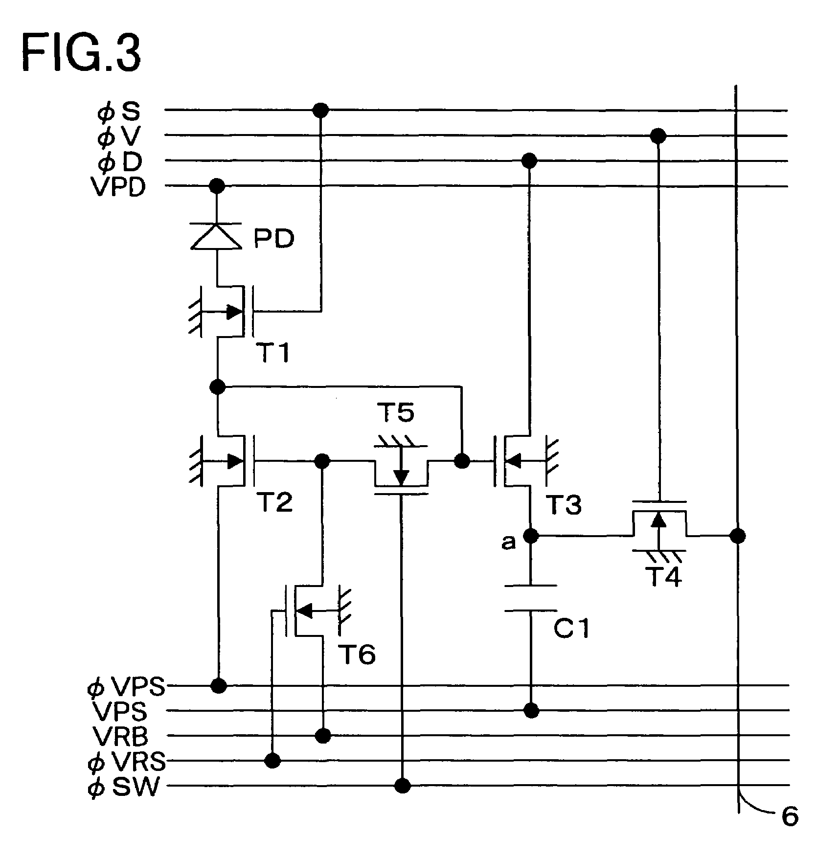
[0118]Now, a first embodiment (FIG. 3) of the invention, which is applicable to each pixel of the first example of the pixel configuration shown in FIG. 2, will be described with reference to the drawings.

[0119]In FIG. 3, a pn photodiode PD serves as a photosensitive element (photoelectric conversion element). The anode of this photodiode PD is connected to the drain of a first MOS transistor T1. The source of this MOS transistor T1 is connected to the drain of a second MOS transistor T2, to the gate of a third MOS transistor T3, and to the drain of the fifth MOS transistor T5. The source of the MOS transistor T3 is connected to the drain of a fourth MOS transistor T4 for selecting a row. The source of this MOS transistor T4 is connected to the output signal line 6 (this output signal line 6 corresponds to the output signal lines 6-1, 6-2, . . . , 6-m in FIG. 2). The MOS transistors T1 to T6 are all N-channel MOS transistors, and have their back gates grounded.

[0120]A direct-current...

second embodiment

[0133]Next, a second embodiment of the invention will be described with reference to the drawings. FIG. 6 is a circuit diagram showing the configuration of each pixel of the solid-state image-sensing device of this embodiment. It is to be noted that such elements, signal lines, and others as are used for the same purposes here as in the pixel shown in FIG. 3 are identified with the same reference symbols, and their detailed descriptions will be omitted.

[0134]As shown in FIG. 6, in this embodiment, the MOS transistors T1 to T5 and the capacitor C1 are configured in the same manner as in the pixel of the first embodiment (FIG. 3), and the only difference is that, instead of the MOS transistor T6 used in the first embodiment, a capacitor C2 is used in this embodiment. Specifically, the capacitor C2 has one end connected to the node between the gate of the MOS transistor T2 and the source of the MOS transistor T5, and receives at the other end the signal φVRS. The signal φVRS is a binar...

third embodiment

[0141]Now, a third embodiment of the invention will be described with reference to the drawings. FIG. 7 is a circuit diagram showing the configuration of each pixel of the solid-state image-sensing device of this embodiment. It is to be noted that such elements, signal lines, and others as are used for the same purposes here as in the pixel shown in FIG. 6 are identified with the same reference symbols, and their detailed descriptions will be omitted.

[0142]As shown in FIG. 7, according to the circuit configuration of this embodiment, as compared with the pixel of the second embodiment (FIG. 6), the MOS transistor T5 is omitted. Specifically, the gates of the MOS transistors T2 and T3 are connected together, and the direct-current voltage VPS is applied to the source of the MOS transistor T2.

(1) How to Convert the Light Incident on the Individual Pixels into an Electric Signal

[0143]In this pixel configured as described above, image sensing is achieved in the same manner as in the sec...


PUM


Abstract

In a solid-state image-sensing device, when image sensing is performed, in each pixel, MOS transistors T1 and T5 are turned on and a MOS transistor T6 is turned off so that a MOS transistor T2 operates in a subthreshold region. When resetting is preformed, in each pixel, the MOS transistors T1 and T5 are turned off and the MOS transistor T6 is turned on so that the gate voltage of the MOS transistor T2 is kept constant. In this state, the MOS transistor T2 is brought first into a conducting state and then, by turning a signal φVPS to a high level, into a cut-off state. This permits a signal proportional to the threshold value of the MOS transistor T2 to be output as compensation data.

Description

[0001]This application is based on applications Nos. H11-208296, H11-272584, and H11-279386 filed in Japan on Jul. 22, 1999, Sep. 27, 1999, and Sep. 30, 1999, respectively, the entire contents of which are hereby incorporated by reference.BACKGROUND OF THE INVENTION[0002]1. Field of the Invention[0003]The present invention relates to an image-sensing apparatus, and particularly to an image-sensing apparatus incorporating a solid-state image-sensing device having a plurality of pixels arranged therein.[0004]2. Description of the Prior Art[0005]Solid-state image-sensing devices designed for use in image-sensing apparatuses are not only small-sized, light-weight, and power-saving, but also free from image distortion, free from image burn-in, and resistant to unfavorable environmental conditions such as vibration and electric fields. Moreover, such image-sensing devices can be manufactured by a process common or analogous to one used to manufacture LSIs (large-scale integrated circuits)...

Claims


Application Information

Patent Timeline
Patent Type & Authority Patents(United States)
IPC IPC(8): H01L31/06H01L31/062H01L27/00H04N5/335H01L27/146H04N5/355H04N5/3745
CPCH01L27/14609H01L27/14643H04N3/155H04N3/1568H04N5/35518H04N5/37452H04N25/573H04N25/771
Inventor HAGIHARA, YOSHIOTAKADA, KENJI
Owner SONY SEMICON SOLUTIONS CORP
Why Eureka
Try Eureka