Semiconductor memory device

a memory device and semiconductor technology, applied in semiconductor devices, digital storage, instruments, etc., can solve problems such as defective products, and achieve the effect of enhancing a production yield

Inactive Publication Date: 2005-09-27
PANASONIC CORP
View PDF3 Cites 15 Cited by
  • Summary
  • Abstract
  • Description
  • Claims
  • Application Information

AI Technical Summary

Benefits of technology

[0022]Therefore, with the foregoing in mind, it is an object of the present invention to provide a semiconduc...

Problems solved by technology

In the case where there is a defect in the dummy cell 512 itself, the amplifier cannot be sta...

Method used


Image

  • Semiconductor memory device
  • Semiconductor memory device
  • Semiconductor memory device

Examples


embodiment 1

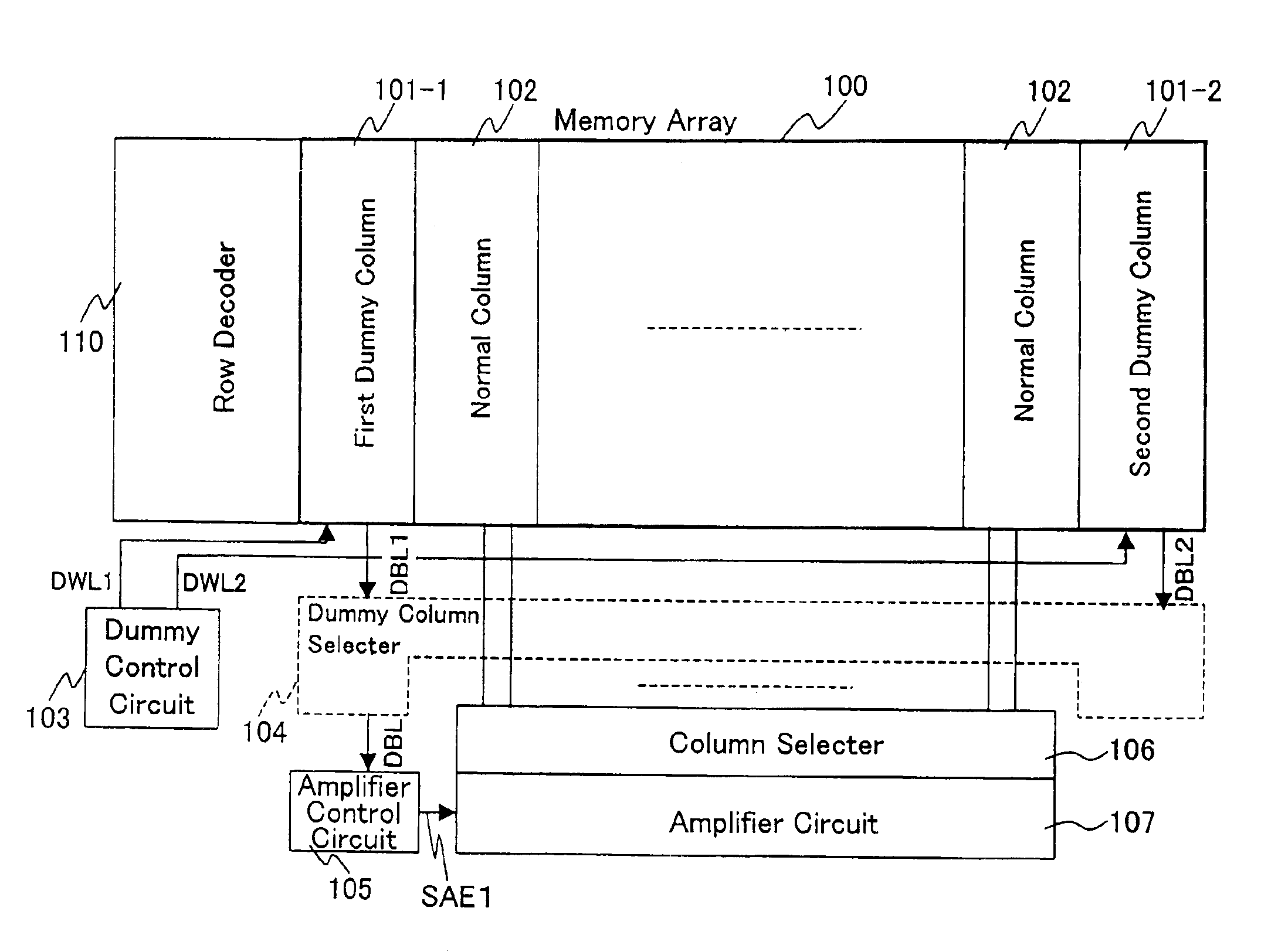
[0067]Hereinafter, a semiconductor memory device according to Embodiment 1 of the present invention will be described with reference to the drawings. FIG. 1 shows an overall configuration of the semiconductor memory device according to Embodiment 1 of the present invention.

[0068]In FIG. 1, reference numeral 100 denotes a memory array, 101-1 denotes a first dummy column that is one of the dummy columns included in two columns in the memory array 100, 101-2 denotes a second dummy column that is the other dummy column, and 102 denotes a plurality of normal columns included in the memory array 100. Herein, the normal columns refer to those columns other than the dummy columns in the memory array 100.

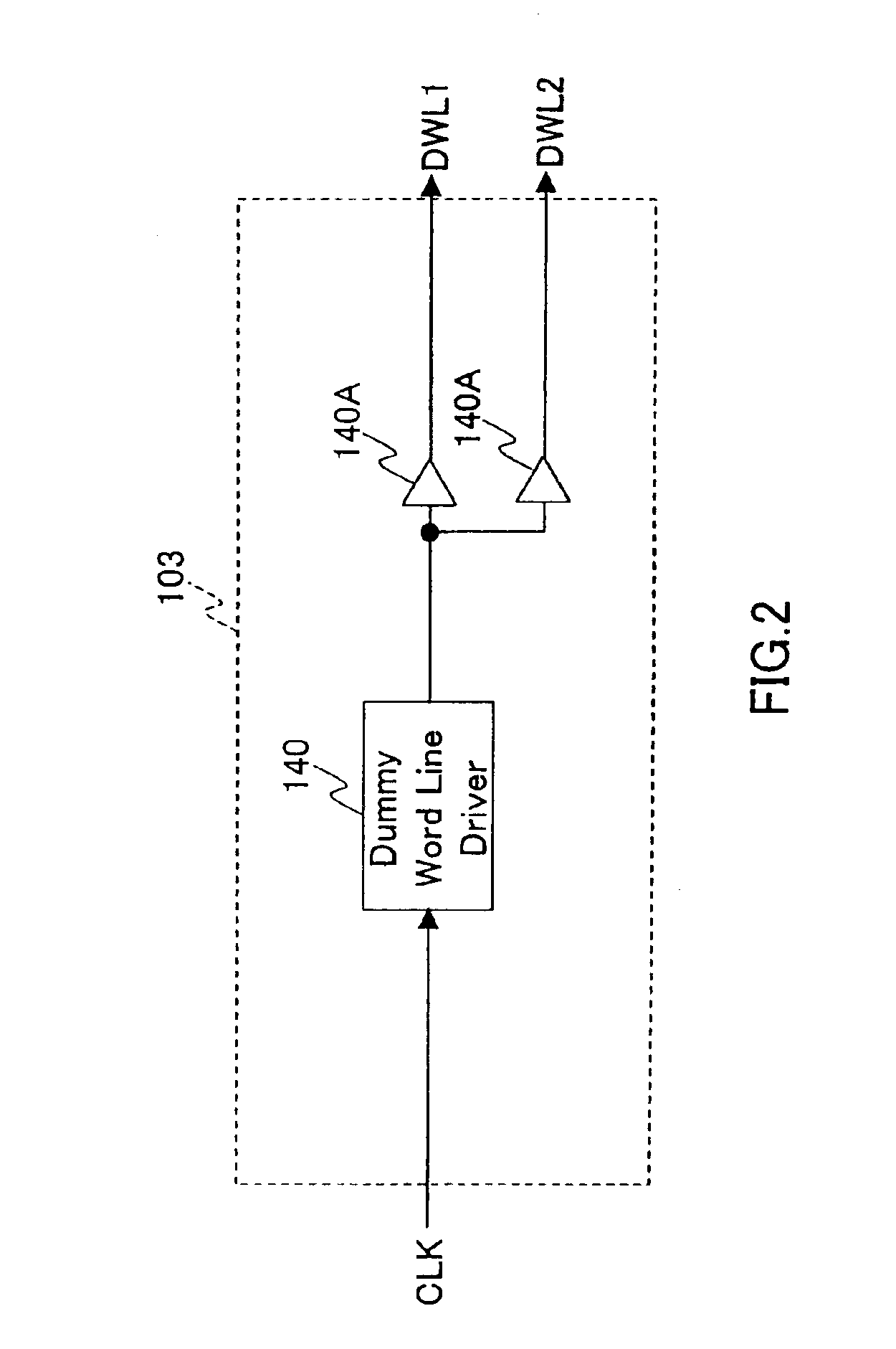
[0069]In Embodiment 1, the first dummy column 101-1 and the second dummy column 101-2 respectively are arranged in a column with the normal columns 102 interposed therebetween. The first dummy column is placed at a position close to the row decoder 110 in a row direction, and the second dumm...

embodiment 2

[0089]Hereinafter, a semiconductor memory device according to Embodiment 2 of the present invention will be described with reference to the drawings. FIG. 9 shows an overall configuration of the semiconductor memory device according to Embodiment 2 of the present invention.

[0090]In FIG. 9, reference numeral 131 denotes a test terminal for measuring the generation of an amplifier startup signal SAE, 203 denotes a dummy control circuit connected to a first dummy column 101-1, a second dummy column 101-2, and a dummy column selector 204, and 204 denotes a dummy column selector connected to outputs of the first dummy column 101-1, the second dummy column 101-2, and the dummy control circuit 203. The remainder of the configuration is the same as that of the semiconductor memory device according to Embodiment 1 shown in FIG. 1. Therefore, like reference numerals denote like components, and the detailed description thereof will be omitted here.

[0091]FIG. 10 shows an internal configuration ...

embodiment 3

[0116]Hereinafter, a semiconductor memory device according to Embodiment 3 of the present invention will be described with reference to the drawings. FIG. 21 shows an overall configuration of the semiconductor memory device according to Embodiment 3 of the present invention. In Embodiment 3, two amplifier control circuits in Embodiment 2 are provided.

[0117]In FIG. 21, reference numeral 300 denotes a memory array, 301-1 denotes a first dummy column that is one of the dummy columns included in two columns in the memory array 300, 301-2 denotes a second dummy column that is the other dummy column, and 303 and 305 denote dummy rows included in the memory array 300, respectively. In Embodiment 3, the dummy columns 301-1 and the second dummy column 301-2 are arranged respectively in a column with normal columns 302 interposed therebetween. The first dummy column 301-1 is placed at a position close to a row decoder 310 in a row direction, and the second dummy column 301-2 is placed at a po...


PUM


Abstract

A semiconductor memory device capable of enhancing a production yield is provided. A dummy control circuit activates a first dummy column including a plurality of dummy cells placed at a position close to a row decoder in a row direction and a second dummy column including a plurality of dummy cells placed at a position farthest from the row decoder in a row direction with a plurality of memory cells interposed between the first dummy column and the second dummy column, through first and second dummy word lines. A dummy column selector selects either one of a signal on a first dummy bit line connected to the first dummy column and a signal on a second dummy bit line connected to the second dummy column, and outputs the selected signal to an amplifier control circuit. The amplifier control circuit generates an amplifier startup signal with respect to an amplifier circuit based on a signal from the dummy column selector.

Description

BACKGROUND OF THE INVENTION[0001]1. Field of the Invention[0002]The present invention relates to a semiconductor memory device for generating a startup timing of an internal circuit by using a dummy circuit. In particular, the present invention relates to a semiconductor memory device capable of relieving a dummy circuit without increasing a chip area to enhance a yield, thereby optimizing a startup timing of an internal circuit.[0003]2. Description of the Related Art[0004]Various methods have been considered for generating a startup signal of an amplifier for amplifying data read from a memory cell by using a dummy memory cell, and allowing the startup timing of the amplifier to precisely follow the variation in read timing of the memory cell caused by a process, a voltage, and the like in a conventional semiconductor memory device.[0005]FIGS. 25 to 28 schematically show circuit configurations disclosed in “IEEE Journal of Solid-State Circuits, Vol. 36, No. 11, November 2001, pp. 1...

Claims


Application Information

Patent Timeline
IPC IPC(8): G11C7/00G11C7/06G11C7/14G11C11/413G11C11/419G11C29/04G11C29/12H01L21/8244H01L27/11
CPCG11C7/06G11C7/14G11C2207/065
Inventor KURUMADA, MAREFUSAAKAMATSU, HIRONORI
Owner PANASONIC CORP
Why Eureka
Try Eureka