Fingerprint sensor package including flexible circuit substrate and associated methods

a flexible circuit substrate and finger contact surface technology, applied in the field of personal identification and verification, can solve the problems of affecting optical sensing, requiring relatively large spacing between the finger contact surface and associated imaging components, and sensors typically requiring precise alignment and complex scanning of optical beams, so as to facilitate electrical interconnection and compact packaging

Inactive Publication Date: 2005-09-27
APPLE INC
View PDF4 Cites 59 Cited by
  • Summary
  • Abstract
  • Description
  • Claims
  • Application Information

AI Technical Summary

Benefits of technology

[0012]This and other objects, features and advantages in accordance with present invention are provided by a fingerprint sensor package comprising a fingerprint sensing integrated circuit in a housing, and a circuit substrate comprising first and second portions connected together, with the first portion being within the housing and mounting the fingerprint sensing integrated circuit, and the second portion being flexible and extending outwardly from the housing for facilitating electrical connection to the fingerprint sensing integrated circuit from external to the housing. Each portion of the circuit substrate preferably includes at least one insulating layer and at least one electrical conductor thereon. Accordingly, the package can be made relatively compact and electrical interconnections are facilitated by the second portion or extension of the circuit substrate. The invention is readily included on the upper surface of a laptop computer, for example.

Problems solved by technology

Unfortunately, optical sensing may be affected by stained fingers or an optical sensor may be deceived by presentation of a photograph or printed image of a fingerprint rather than a true live fingerprint.
In addition, optical schemes may require relatively large spacings between the finger contact surface and associated imaging components.
Moreover, such sensors typically require precise alignment and complex scanning of optical beams.
Accordingly, optical sensors may thus be bulky and be susceptible to shock, vibration and surface contamination.
Accordingly, an optical fingerprint sensor may be unreliable in service in addition to being bulky and relatively expensive due to optics and moving parts.
Unfortunately, the resilient materials required for the sensor may suffer from long term reliability problems.
In addition, multiplexing techniques for driving and scanning each of the individual capacitors may be relatively slow and cumbersome.
Moreover, noise and stray capacitances may adversely affect the plurality of relatively small and closely spaced capacitors.
Unfortunately for many applications, it may not be inconvenient to connect the sensor directly onto a conventional motherboard, for example.
This is especially the case in a laptop computer, for example, where direct connection to a motherboard is not practical, and available mounting space is at a premium.
Yet another disadvantage with the conventional packaging is that the finger of the user may be uncomfortably bent backwards to permit the fingertip to be positioned on the flat sensor surface.

Method used


Image

  • Fingerprint sensor package including flexible circuit substrate and associated methods
  • Fingerprint sensor package including flexible circuit substrate and associated methods
  • Fingerprint sensor package including flexible circuit substrate and associated methods

Examples


Embodiment Construction

[0028]The present invention will now be described more fully hereinafter with reference to the accompanying drawings, in which preferred embodiments of the invention are shown. This invention may, however, be embodied in many different forms and should not be construed as limited to the embodiments set forth herein. Rather, these embodiments are provided so that this disclosure will be thorough and complete, and will fully convey the scope of the invention to those skilled in the art. Like numbers refer to like elements throughout, and prime notation is used to indicate similar elements in different embodiments. The scaling of various features, particularly layers in the drawing figures, have been exaggerated for clarity of explanation.

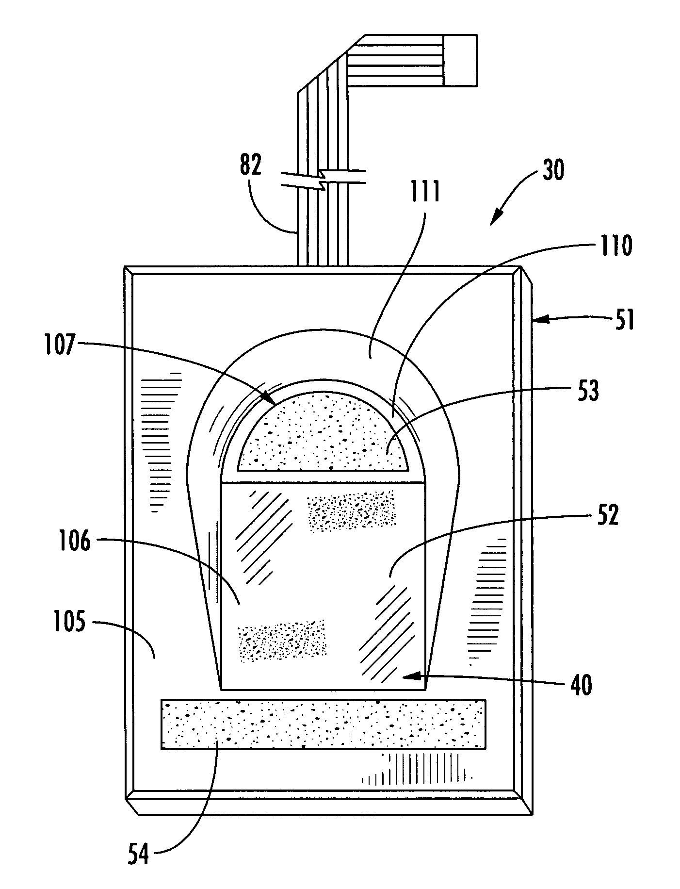
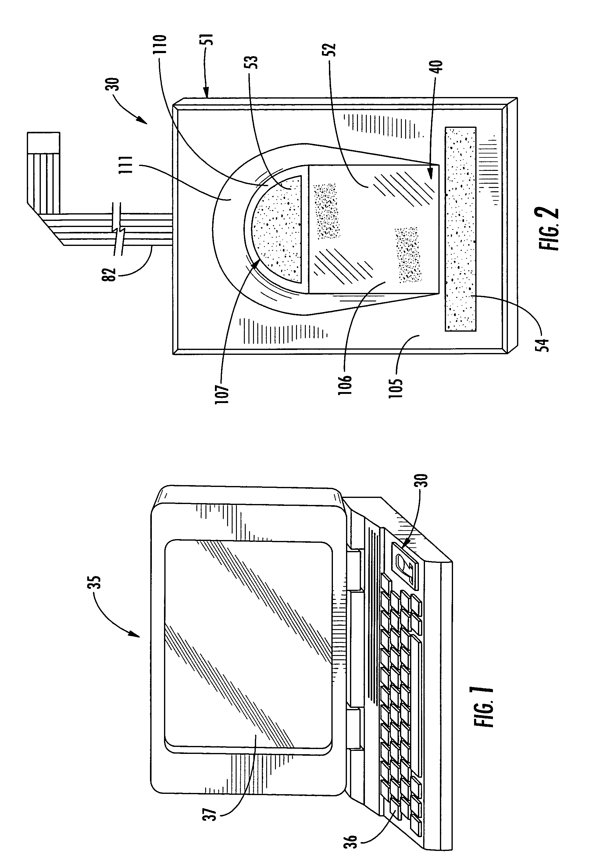
[0029]Referring to FIGS. 1–4, the fingerprint sensor package 30 in accordance with the invention is initially described. As shown in FIG. 1, the sensor package 30 is especially suited for certain applications, such as mounted in a laptop computer 35. ...


PUM


Abstract

A fingerprint sensor package preferably includes a fingerprint sensing integrated circuit in a housing, and a circuit substrate comprising first and second portions connected together. The first portion is within the housing and mounts the fingerprint sensing integrated circuit, and the second portion is flexible and extends outwardly from the housing for facilitating electrical connection to the fingerprint sensing integrated circuit from external to the housing. Each portion of the circuit substrate preferably includes at least one insulating layer and at least one electrical conductor thereon. Accordingly, the package can be made relatively compact and electrical interconnections are facilitated by the second portion or extension of the circuit substrate. In one embodiment, the first and second portions are integrally formed together. In this embodiment, the first portion is also flexible. The sensor package is readily included on the upper surface of a laptop computer, for example.

Description

RELATED APPLICATION[0001]This application is based upon prior filed copending provisional application Ser. No. 60 / 133,626 filed May 11, 1999.FIELD OF THE INVENTION[0002]The present invention relates to the field of personal identification and verification, and, more particularly, to the field of fingerprint sensing and processing.BACKGROUND OF THE INVENTION[0003]Fingerprint sensing and matching is a reliable and widely used technique for personal identification or verification. In particular, a common approach to fingerprint identification involves scanning a sample fingerprint or an image thereof and storing the image and / or unique characteristics of the fingerprint image. The characteristics of a sample fingerprint may be compared to information for reference fingerprints already in a database to determine proper identification of a person, such as for verification purposes.[0004]A typical electronic fingerprint sensor is based upon illuminating the finger surface using visible li...

Claims


Application Information

Patent Timeline
Patent Type & Authority Patents(United States)
IPC IPC(8): G06K9/00
CPCG06K9/0002G06V40/1306
Inventor SETLAK, DALE R.WILLIAMS, DARYL
Owner APPLE INC
Why Eureka
Try Eureka