ECC circuit-containing semiconductor memory device and method of testing the same

a technology memory device, which is applied in the direction of error detection/correction, redundant data error correction, instruments, etc., can solve the problems of increasing the probability of error write and error read, the inability to quickly carry out test, and the inability to meet the demand for compactness of electronic equipment. , to achieve the effect of improving the reliability of ecc circuit-containing semiconductor memory device, high performance and simplified structur

Inactive Publication Date: 2005-08-30
PANASONIC CORP
View PDF15 Cites 38 Cited by
  • Summary
  • Abstract
  • Description
  • Claims
  • Application Information

AI Technical Summary

Benefits of technology

[0030]An object of the invention is providing a semiconductor memory device containing an ECC circuit with a simplified structure which can exhibit high performance suitable to compactness of electronic equipment for mounting the semiconductor memory device, and providing a test method for improving the reliability of the ECC circuit-containing semiconductor memory device.
[0032]In this manner, an error correcting code generating circuit and a decoder, which are separately provided in the conventional technique, can be constructed by using the shared circuit. As a result, the semiconductor memory device can be made compact.
[0034]In this manner, the semiconductor memory device can be provided with a function to detect a defect or the like derived from interference or the like between adjacent memory cells in each storage means by generating a checker pattern and a stripe pattern without additionally preparing error correcting code patterns for memory test.
[0036]In this manner, a defect of the decoding means can be detected, resulting in further improving the reliability of the ECC circuit-containing semiconductor memory device.

Problems solved by technology

In accordance with recent increase in the storage capacity of a semiconductor memory device, the probability of failure occurring in any of memory elements included in the semiconductor memory device or the probability of error write and error read has been increased.
In the first conventional example, in the case where different test patterns (such as a checker pattern) should be respectively used for testing the data storage area and the error correcting code storage area, the test cannot be rapidly carried out.
Therefore, it is difficult to sufficiently meet demand for compactness of electronic equipment including the semiconductor memory device.
Furthermore, in the structure shown in FIG. 10 or 11, there is no means for testing an operation for correcting an error of the decoder 105, and there is a possibility that a 1-bit error cannot be accurately corrected.
In other words, the reliability of an ECC circuit-containing semiconductor memory device cannot be sufficiently guaranteed by the conventional test method.

Method used


Image

  • ECC circuit-containing semiconductor memory device and method of testing the same
  • ECC circuit-containing semiconductor memory device and method of testing the same
  • ECC circuit-containing semiconductor memory device and method of testing the same

Examples


embodiment 1

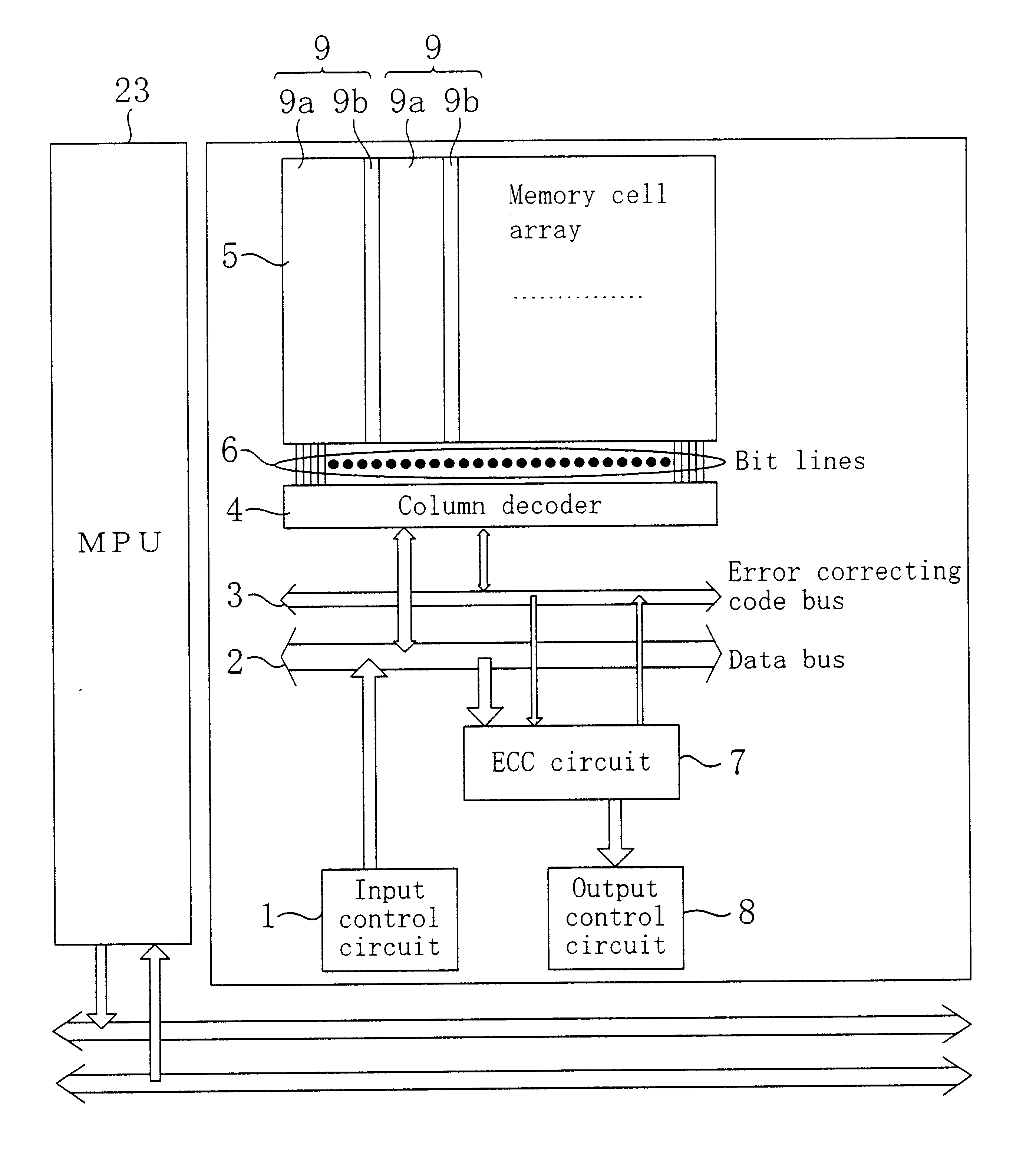
[0060]FIG. 1 is a block diagram for schematically showing the structure of an ECC circuit-containing semiconductor memory device according to Embodiment 1 of the invention. As is shown in FIG. 1, the semiconductor memory device includes a memory cell array 5 where a large number of memory cells are arranged in the form of a matrix, and the memory cell array 5 is divided into plural memory blocks 9. Each memory block 9 includes a data storage area 9a and an error correcting code storage area 9b as is shown in FIG. 4. In the periphery of the memory cell array 5, a column decoder 4 for selecting a column and a row decoder (not shown) for selecting a row are disposed. The column decoder 4 and the row decoder are connected to the memory cell array 5 through a bit line group 6 and a word line group (not shown), respectively. Circuits provided to the row decoder are not concerned with the characteristics of the invention and hence are omitted in FIG. 1.

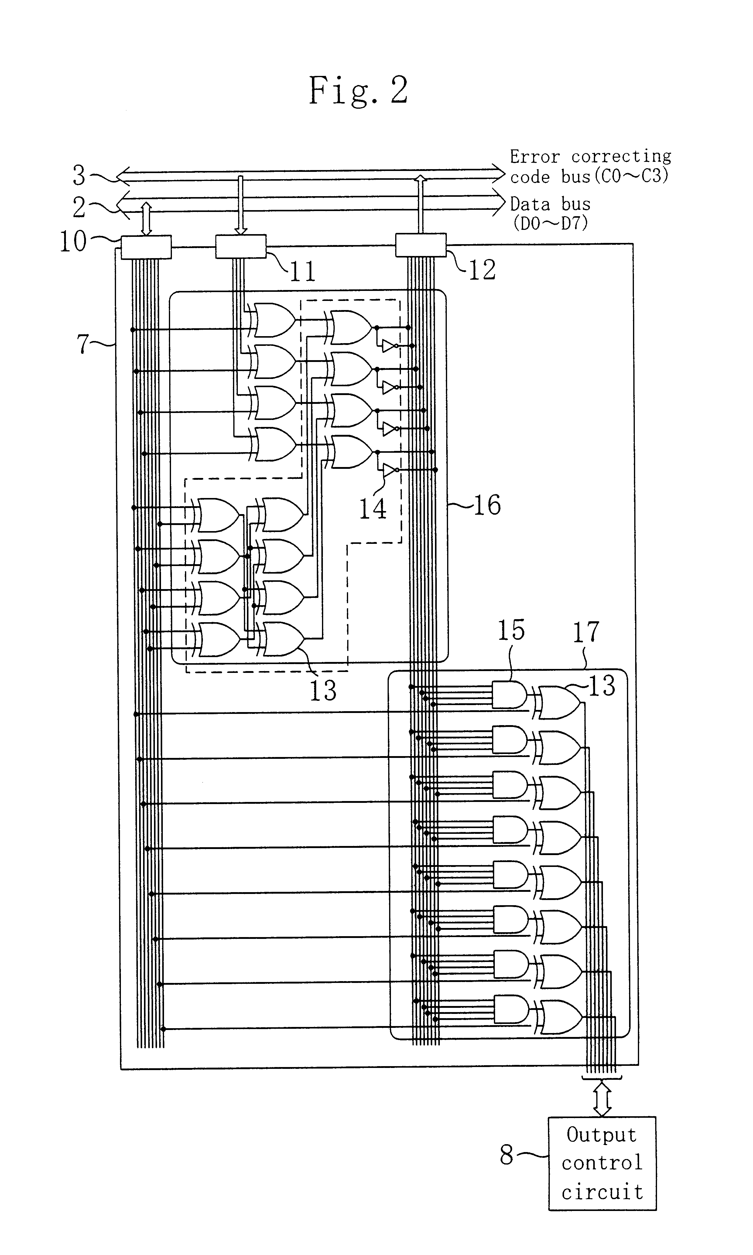
[0061]Main peripheral circuits are an...

embodiment 2

[0093]FIG. 4 is a diagram for schematically showing the structure of a memory cell array 5 of an ECC circuit-containing semiconductor memory device according to Embodiment 2 of the invention. As is shown in FIG. 4, the memory cell array 5 is divided into four memory blocks 9, each of which includes a data storage area 9a and an error correcting code storage area 9b. The row number in the memory cell array 5 is indicated as X (=0, 1, 2, . . . or 255), and the number of each memory block 9 is indicated as Y (=0, 1, 2 or 3). The data storage area 9a and the error correcting code storage area 9b of each memory block 9 together serve as a memory cell block corresponding to one word, and this memory block corresponding to one word is designated as a “unit word block”.

[0094]It is assumed also in this embodiment that a 4-bit error correcting code is generated from an 8-bit data by using Formulas (3) described in Embodiment 1. In other words, this embodiment is also characterized by generati...

embodiment 3

[0104]FIG. 6 is a block diagram for showing the structure of an ECC circuit-containing semiconductor memory device according to Embodiment 3 of the invention.

[0105]As is shown in FIG. 6, the structure of the ECC circuit-containing semiconductor memory device of this embodiment is substantially the same as that of Embodiment 1 (shown in FIG. 1). The structure of this embodiment additionally includes a test circuit 22 for conducting a memory test by outputting a test pattern to the input control circuit 1 of the ECC circuit-containing semiconductor memory device and inputting the test pattern from the output control circuit 8, and this embodiment is characterized by a test method employed by this test circuit 22.

[0106]As described with respect to the conventional technique, in an ECC circuit-containing memory device capable of correcting a 1-bit error, in order to conduct a memory test without using a signal line for inputting / outputting an error correcting code between an ECC circuit...


PUM


Abstract

In an ECC circuit of an ECC circuit-containing semiconductor memory device, an error correcting code / syndrome generating circuit and a data correcting circuit are disposed. In portions of the ECC circuit connected to buses, a data bus input control circuit for controlling input of a data from a data bus; an error correcting code bus input control circuit for controlling input of an error correcting code from an error correcting code bus; and an error correcting code bus output control circuit for controlling output of an error correcting code to the error correcting code bus are disposed. A portion corresponding to an error correcting code generator of a conventional technique is included in the ECC circuit, so that the ECC circuit can function both as an error correcting code generator and a decoder. As a result, the entire device can be made compact.

Description

BACKGROUND OF THE INVENTION[0001]The present invention relates to a semiconductor memory device containing an error correcting code circuit (ECC circuit).[0002]In accordance with recent increase in the storage capacity of a semiconductor memory device, the probability of failure occurring in any of memory elements included in the semiconductor memory device or the probability of error write and error read has been increased. Therefore, an ECC circuit-containing semiconductor memory device having a function to detect a data error from an electric signal and correct the detected error has been proposed.[0003]An ECC circuit has an error correcting function designed on the basis of a coding theory. An error is corrected through encoding as follows: Information to be originally transferred is sent with redundancy added in accordance with a given rule, and a receiver checks whether or not the received information accords with the rule, so as to detect and correct an error in accordance wi...

Claims


Application Information

Patent Timeline
Patent Type & Authority Patents(United States)
IPC IPC(8): G06F11/10G11C29/42G11C29/04G11C29/02
CPCG06F11/1008G06F11/102G06F11/2215G11C29/02G11C29/42
Inventor HONDA, TOSHIYUKI
Owner PANASONIC CORP
Why Eureka
Try Eureka