Correlation of electrical test data with physical defect data

a technology of electrical test data and correlation, applied in the direction of resistance/reactance/impedence, testing circuit, instruments, etc., can solve the problems of poor device or circuit-level functional characteristics, difficult detection of physical defects, time-consuming and expensive failure analysis techniques, etc., to improve yield analysis

Active Publication Date: 2005-09-27
XILINX INC
View PDF1 Cites 403 Cited by
  • Summary
  • Abstract
  • Description
  • Claims
  • Application Information

AI Technical Summary

Benefits of technology

[0006]Various methods are disclosed for analyzing yield data produced in testing a semiconductor chip. The electrical data is translated into a physical location de

Problems solved by technology

Poor device or circuit-level functional characteristics may be caused by physical defects.
However, physical defects may be difficult to detect after manufacture of the chip is complete.
However, failur

Method used


Image

  • Correlation of electrical test data with physical defect data
  • Correlation of electrical test data with physical defect data
  • Correlation of electrical test data with physical defect data

Examples


Embodiment Construction

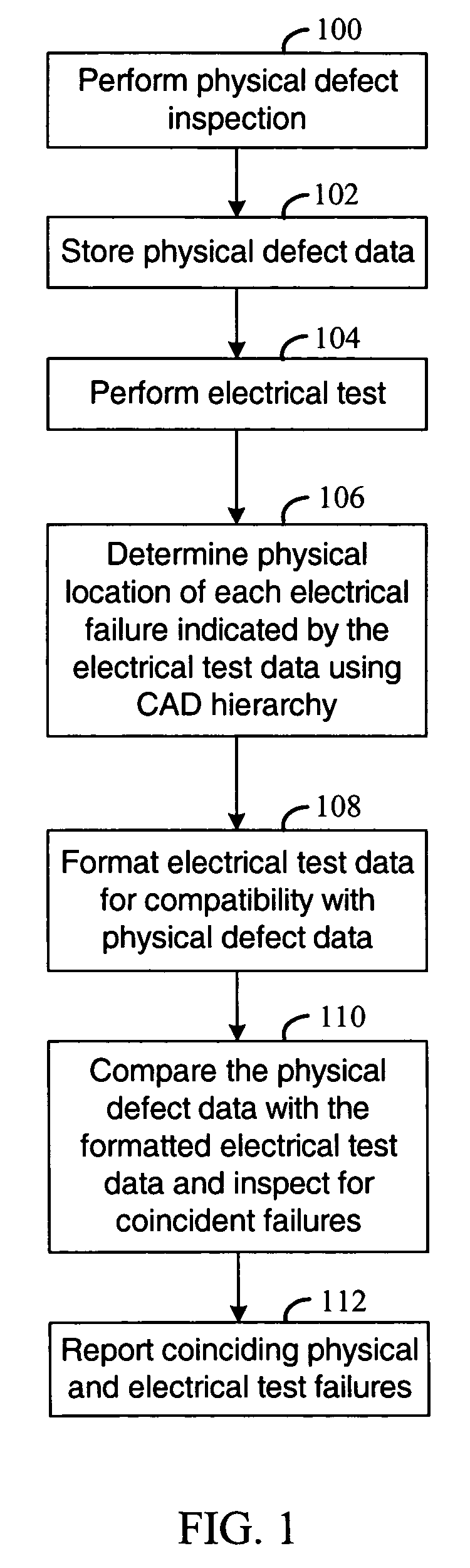
[0016]FIG. 1 is a flowchart of an example process for analyzing data generated in testing a semiconductor chip in accordance with various embodiments of the invention. During manufacture of the chip, various inspections are performed in an attempt to find physical defects (step 100). This process may be referred to as “in-line” inspection. Various known techniques may be used to inspect the chip. For example, inspection techniques that use an electron / ion beam, lasers, or various other optical apparatus may be used for physical inspection. Data gathered during in-line inspection and associated with physical defects are stored for later analysis (step 102).

[0017]Electrical testing may be performed at some time after manufacture of the chip is complete and test data generated from the testing is stored for subsequent analysis (step 104). Data associated with a failure(s) detected during electrical testing are analyzed to determine the physical location(s) of failing circuit elements (...


PUM


Abstract

Method and apparatus are disclosed for analyzing defect data produced in testing a semiconductor chip from a logic design. In various embodiments, input for processing is a first inspection data set that identifies a first set of physical locations that are associated with defects detected during fabrication of the chip. Also input is a second test data set that includes one or more identifiers associated with failing circuitry in the chip. A second set of physical locations is determined from the one or more identifiers of failing circuitry, hierarchical relationships between blocks of the design, and placement information associated with the blocks. Each of the one or more identifiers is associated with at least one of the blocks. Correspondences are identified between physical locations in the first inspection data set and the second set of physical locations.

Description

FIELD OF THE INVENTION[0001]The present invention relates in general to semiconductor chip defect analysis.BACKGROUND OF THE INVENTION[0002]Semiconductor chip manufacturing requires defect analysis to help improve chip yield and monitor the production environment. Semiconductor chips are tested for the presence of physical defects at various processing steps during the manufacturing process. “In-line” measurements occur while the semiconductor chips are within the fabrication facility. Example physical defects include pinholes, voids, spikes, or agglomerations. With the aid of defect data analysis, equipment failure or fabrication facility contamination may be inferred.[0003]Electrical measurements may be taken and further analysis performed after completing manufacture of the semiconductor chip. The electrical measurements, which produce electrical test data, or “electrical data” for short, and analysis may help improve chip yield and provide information in support of monitoring th...

Claims


Application Information

Patent Timeline
IPC IPC(8): G01R31/00G01R31/28G01R31/3185G11C29/44
CPCG01R31/2894G11C29/44G01R31/318566G11C2029/1806
Inventor FAN, YUEZHENXU, JASONTANG, STEPHEN WING-HOLING, ZHI-MIN
Owner XILINX INC
Why Eureka
Try Eureka